Impressive progress 🙂
How did you soldered the TAS3251 once c17 and c9 removed ? How do you rate the difficulty ?
I'm really impressed by your software developpement. You developped quite complex function very fast.
Hope that you will be able to do the sound tests soon.
You have set resistors at the output ? Which values and which power rating ?
Well done 🙂
JMF
To solder the TAS I applied the same method I use for such low pin pitch chip:
As soon I’ll have a functional V0, I’ll make the binaries available for the builders of this project. Loading the software is very easy with free ST software and a 2USD STLink.
For the resistors I do not intend to do some power testing with those. I’ve installed them because as far as I know those Class D amp needs to be loaded in order to damp their high Q LC output filter and avoid destroying output stage. Not sure if it’s really required, I’ll check later in TAS DS, for now it’s a safety measure. But that’ll be useful for low power tests. Higher power tests will first require building a heatsink for the TAS.
- Carefully apply paste with a small screwdriver, remove all excess. If paste is too dry, slightly preheat the chip area.
- Place the chip and solder it with hot air gun.
- Clean all the pins with fresh solder braid, section perpendicular to the pin axe (that’s why I removed the caps) and a flat soldering iron tip.
- As my paste is a bit old and dry, it tends to form small balls so I generously apply flux on the chip and strongly reheat it applying air flow between the leads to avoid bridge under the chip
- Have visual inspection for each step. Having good lens is required, if not some smartphone may help with lens software and their powerful led
- Clean the board with IPA
- Power up with current limiting supply…
As soon I’ll have a functional V0, I’ll make the binaries available for the builders of this project. Loading the software is very easy with free ST software and a 2USD STLink.
For the resistors I do not intend to do some power testing with those. I’ve installed them because as far as I know those Class D amp needs to be loaded in order to damp their high Q LC output filter and avoid destroying output stage. Not sure if it’s really required, I’ll check later in TAS DS, for now it’s a safety measure. But that’ll be useful for low power tests. Higher power tests will first require building a heatsink for the TAS.
Quick update
Lots of debugging around the command parser then around the TAS I2C loader has been done. It has finally been solved with a logic analyser and I now have evidence the TAS receive and handle the right data.
I also encountered issue around C19, which is the charge pump cap : unsoldered it , cleaned it up, reinstalled it, reheated and cleaned up corresponding TAS pins, now it’s ok, -3,3V is generated when TAS received an I2S signal.
Despite these progress, there’s still no sound, DAC remains muted. I suspect a clock error and have to monitor the clock error status registers and try another I2S source.
There are plenty off errors in the datasheet, some text chunks are cut/paste from another chip DS and are not relevant : typically the config scripts examples. Fortunately, PPC3 generated scripts are ok even if they use defaults some default setting. There’s also TI E2E community, which provide some valuables clues not in the datasheet.
I continue digging...
What is your current startup procedure?
To test basic functionality you dont have to load a DSP file. You can boot up, apply I2S and set it to normal operation (0x02 = 0). It should play sound that way. Also handy to add a "status" command to your parsers so you can request all status/error/fault registers in one go to see what is going on
To test basic functionality you dont have to load a DSP file. You can boot up, apply I2S and set it to normal operation (0x02 = 0). It should play sound that way. Also handy to add a "status" command to your parsers so you can request all status/error/fault registers in one go to see what is going on
Startup script is an extract from the basic stereo 48k process flow of PPC3, adjusted to run 32b I2S data as default is 24. My I2S source is an AK4113 running 32b.
Script effectively start the DAC & DSP : it has external consequences which confirm that the right parameters are loaded at the right place. For example : the charge pump starts and SDOUT provides the result define by the configuration data.
I'll write this evening the code aiming at displaying the relevant registers, this should bring me some light and will try without any DSP coeff loaded.
Thanks
Sorry to learn that you have difficulties generating sound. I managed to recover today the equipment I'm missing to finalize the boards and benefit from the 2 coming long week-ends to progress.
I have the basic Arduino code to make the board alive running on a Bluepill. But still have to develop the stm32F030C8 variant. I also have a USB to I2S board that I never tried before.
I hope to catch up with your status next week. Hope to be able to bring more information.
JM
I have the basic Arduino code to make the board alive running on a Bluepill. But still have to develop the stm32F030C8 variant. I also have a USB to I2S board that I never tried before.
I hope to catch up with your status next week. Hope to be able to bring more information.
JM
Now it produce some sound !. Basics test with a test speaker and my lab supply are very promising, the amp seems very powerful, and sounds sharp and clear.
I encountered various issues and I still have some, but this not surprising: this is a new chip, a new software and new pcb, this make a strong probability to meet issues combined with those 3 factors…
First I had some soldering issues, which generated some erratic behaviour of the DAC, DSP and power amp. I had to remove the chip then to solder it back while adding flux to my solder paste which is definitely too old and dry.
I also had DC offset on output (~500mV) : the four ecap between the DAC and the power amp where leaking because they were reverse biased due to a silkscreen mismatch.
The last remaining issue is related to the setup of the chip. Setup could be applied one time only after a cold start. If a re-apply it or apply a new one the output vanish. Only a cold start allow to recover output.
I’ll continue digging, I now have a software way to display the status register of the chip I should find an error flag somewhere…
Good news !
I'm really sorry for the mistake on those caps. Initially it was not polarised X7R caps, and I did not paid enough attention to the polarity when I changed them for audio grade electrolytics. Hopefully you found the error. I will correct the silkscreen (and with other suggestions you would have).
I have now borrowed the missing equipment I missed, so I resume my work. Started yesterday to populate the 0805. I stoppes at the L5 power supply self, for which I have difficulies with my soldering iron. I will try with hot air this evening.
JMF
So, now a second board is on the workbench:
- additional SMD components soldered, except TAS3251 itself,
- 15V, 12V and 3.3V power supply stages working,
- stm32 operational with blink code.
Next stage is to implement a "NeatAmp variant" in the Arduino environment and be able to download applications developped in the Arduino IDE.
JMF
- additional SMD components soldered, except TAS3251 itself,
- 15V, 12V and 3.3V power supply stages working,
- stm32 operational with blink code.
Next stage is to implement a "NeatAmp variant" in the Arduino environment and be able to download applications developped in the Arduino IDE.
JMF
Is there a reason why most designs go for 15V first, and then 12 and 3.3V? Is it noise? Im working on a TAS3251 design too and am looking at the options. Are your schematics available somewhere?
Today update : It works !.
The issue related to configs requiring cold boot is solved, it seems that DAC_MUTE should be set low during config update (not DSP coeff, only config). As the chip doesn’t have a hardware reset pin, having DAC_MUTE low seem to be required to have the soft reset (Reg01) operate properly.
I also encounter some software related issues regarding I2C write to TAS. TAS has to be managed as a I2C memory device.
But the reason why I lost the most time is that the default configuration provided by PPC3 I used (standard stereo 48k) doesn't work, at least on the DSP part with the biquad coefficients, the gains seem to be set to zero and it produce nothing. Besides it doesn't even match the application note on process flows (SLAA799A).I finished by writing by hand a very simple biquad config (volume control) which confirm software and TAS is ok.
Volume control using a pot has been implemented, it needs calibration: the TAS play very loud and there’re many (at least 3) volume control stage in the signal path. The analog one (0/-6dB selector) and the basic digital one (Reg0x3D-3E, B0/P0) are documented but not the one to use (Reg0x44-0x48, Page x01e) within the biquads area. Question : which balance for the best dynamique and SNR ?. For now I have -6dB analogic, -44dB digital, +24dB default TAS gain and my volume control based on Reg0x44 and 0x48 biquads.
Still few bugs to remove and first version of software is mainly ready.
More tomorrow
Attachments

Is there a reason why most designs go for 15V first, and then 12 and 3.3V? Is it noise? Im working on a TAS3251 design too and am looking at the options. Are your schematics available somewhere?
I had same question.
In fact thats what is made in the EVM.
On EVM, the 15V produced by the LM5010 is not very clean, I get up to 100mV of ripple (our board is a copy of EVM supply section) . It's may be required to have a clean 12V for gate drive produced by a linear regulator. As amp supply may goes to 36V, a 12V linear will have to dissipate a lot of power, so a switching pre regulator may be relevant.
Hello,
My explanation of the 15V step is that it is done like that in the TI EVM board. Doctormord had in mind it could be skipped. But I didn't dared to do it. However it is not an expensive part.
Schematics could be available in an Open Hardware spirit. I put on the board CC-BY-SA 4.0. Don't know it it fits your intention.
This license lets others remix, adapt, and build upon your work even for commercial purposes, as long as they credit you and license their new creations under the identical terms. This license is often compared to “copyleft” free and open source software licenses. All new works based on yours will carry the same license, so any derivatives will also allow commercial use. This is the license used by Wikipedia, and is recommended for materials that would benefit from incorporating content from Wikipedia and similarly licensed projects.
JMF
Today update : It works !.
The issue related to configs requiring cold boot is solved, it seems that DAC_MUTE should be set low during config update (not DSP coeff, only config). As the chip doesn’t have a hardware reset pin, having DAC_MUTE low seem to be required to have the soft reset (Reg01) operate properly.
I also encounter some software related issues regarding I2C write to TAS. TAS has to be managed as a I2C memory device.
But the reason why I lost the most time is that the default configuration provided by PPC3 I used (standard stereo 48k) doesn't work, at least on the DSP part with the biquad coefficients, the gains seem to be set to zero and it produce nothing. Besides it doesn't even match the application note on process flows (SLAA799A).I finished by writing by hand a very simple biquad config (volume control) which confirm software and TAS is ok.
Volume control using a pot has been implemented, it needs calibration: the TAS play very loud and there’re many (at least 3) volume control stage in the signal path. The analog one (0/-6dB selector) and the basic digital one (Reg0x3D-3E, B0/P0) are documented but not the one to use (Reg0x44-0x48, Page x01e) within the biquads area. Question : which balance for the best dynamique and SNR ?. For now I have -6dB analogic, -44dB digital, +24dB default TAS gain and my volume control based on Reg0x44 and 0x48 biquads.
Still few bugs to remove and first version of software is mainly ready.
More tomorrow
Very happy that it works 🙂 Well done AIM65 !!!
I'm surprised about all those glitches in the TI documentation and the files produced by PPC3 :-(
You still run the board without heatsink, with a (small) loudspeaker ? How much voltage amplitude do you have at the output ?
JMF
Hi Jean-Marc,
First, thanks for given us such an interesting project. A lot to learn, to test/try and to obtain results !
Speaking results, for now, the little chip give surprising results on my crappy, plastic made, Sony speaker. I can't wait to test them on real speakers.
About heat sink, well spotted !, I’ll make something tomorrow, for now I place a part of “duralumin” on the chip when playing music. I do not play loud for long time, so it’s alright and the onboard FAULT led says when party has to be terminated !..
When playing loud, I’ll go to clipping (led lights on, I’ll measure tomorrow but DS says that rail 2 rail is achievable.)
I’ll fix tomorrow some bug and prepare some description of the software.
Christophe, your specification advices helped make this board more versatile and suitable for many projects. This is a good thing.
On my side, I have the first results about the Arduino variant. I can download the sketch from the Arduino IDE. As of today, the outputs are working (LED, Reset_Amp).
I will solder additional pinheads tomorrow, to check the good operation of:
- the Digital inputs
- the Analog inputs
- the I2S_1 (the one that will control the TAS3251)
- the I2S_2 (the one that also address the EEPROM
- if I can build a serial monitor with an arduino board, I will try to test the Serial interface.
JMF
So, the Arduino implementation seems to work correctly.
I could actuate:
- the Digital inputs
- the Analog inputs (Voltage measure and Volume pot)
- the I2C_1 (the one that will control the TAS3251 and address the EEPROM)
- the I2C_2 (additional one)
- the serial interface (to "print" from the uC to the logic analyser).
For the I2C they are alive with the logic analyser, but I failed to buid a working slave with the ESP8266 and ESP32. Seems thate there is code only for Master. I also have an arduino, but did nout used it as it is 5V and the stm32F030C8 is not 5V tolerant.
Note that the I2C2 needs external pull-up to work
So... next stage is soldering the TAS3251. I will use a mini stencil made from mylar sheet and laser cutter.
JMF
Last edited:
Awesome work, Jean-Marc and Christophe - watching your efforts
with great interest. Appreciate the board being released under CC-BY-SA 4.0 license.
Looking forward to the final result 🙂
with great interest. Appreciate the board being released under CC-BY-SA 4.0 license.
Looking forward to the final result 🙂
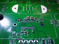
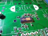
So yersterday, I soldered the TAS3251. The "mini stencil" strategy looks to have worked. Solder paste and hot air look magic to my eyes.
Have to double check before powering.
Have to double check before powering.
Attachments

So yersterday, I soldered the TAS3251. The "mini stencil" strategy looks to have worked. Solder paste and hot air look magic to my eyes.
Have to double check before powering.
Hi,
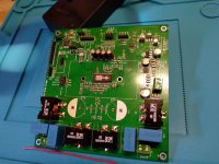
I just took a quick look on the pictures of your PCBs and the layout recommendations in the tas3251 datasheet.
On the first view that reference design doesn't really look that well thought out. I think the routing could be improved. Especially because the chip doesn't have a power pad on the bottom side.
Those vias routing the amp outputs to bottom in the datasheet are rather of a symbolic value. I think that should symbolise that there will be vias needed. Those 5 vias will not really be capable of handling 175 W per channel. I think you should use much more vias or filled ones or what would be the best, route the power lines on top without vias to bottom.
- Home
- Amplifiers
- Class D
- [design log] Neat 2x170W I2S in, I2C controlled, integrated DSP amp (TAS3251)