No prbolem, i'm in the same situation.Once again my apologies for the delay in replying, this week has somehow been very busy for me.
Correct, but there are two items : large resistance is placed between the HV-supply and the membrane to get a constant charge system, which is also safer in case the membrane runs into the stators (smaller charge is less likely to damage the fragile membrane) and also as a current limite in case of skin contact (mostly the HV-supply cascades are such low-current diveces that this not to big of a problem. HV transformers of neon lights are another story).My understanding is that one uses a large value resistor to minimize the current to the membrane film power supply, and to avoid the prospect of death if one accidently touched it.
But to achieve current drive in stead of voltage drive, large resistors are (sometimes) included between step-trafo and the stators (so in the audio signal). This is done to make the ESL work according to the formula of Peter Walker to achieve flat FR. So these resistors are used, for one or more of the following :
1. create or approche constant current drive
2. limit the drive current on the stators (since these are more exposed and drive by a amp, there is more danger if one touches a stator (although they are mostly insulated) while playing loud.
3. Reduce or control some HF resonance in the step-up transformer
4. increase the impedance as seen by the amp to a more friendly value of at least 2 to 3 Ohms.
5. In case of a segmented ESL panel it can be used as a RC filter to tune the FR between the sections.
So it is not always clear which function
For the moment I have wound 2 step-up transformers on c-cores based on a description of Mark Schroeyers on the Audio-circuits (designed for a normal, complicated amp with lots of components). The primaries are quadfilar wound (4x0.4mm). THese 4 are connected in parrallel for the moment (It must be possible to centre tap between the 2 bobins). Secondary is a single 0.1 mm wire. Step-up ratio 1:108.If you bifilar wind the primaries then you can use the transformer in PP directly from the mosfets.
I'am not yet working on the amp, but i'm tempted to give it a try this summer. The PS for the amp can remain +35 V i suppose.What power supply voltage are you using for the amp?
I am going to try a HV-supply of max 15 KV (membrane/stator is > 6mm). I have ordered some HV-supplies in the U.S. but air-mail is already 3 weeks on its way, so I cannot start testing my prototype.What power supply voltage are you using for the amp?
6KV (the more the better)What PP voltage across the plates are you aiming for?
No, but a double bobin on the c-core (su75b gos 0.3mm)Are you using a dual chamber bobbin
For the moment, each bobin has 5 sections (P-S-P-S-P), the 2 bobbins are placed in series, so totatl 10 sections. Construction similar (at least I hope) as Lundahl.How many layer sections are you looking at?
Well, for the moment i am at 1:108 for an amp that can deliver 20Vrms max. Most esl step-ups work with a total step-up of 1:70 up to 1:240. I was kind of hoping that with your amp and a rail voltage of max 50 V, I could lower the step-up ratio to make it easier to keep a large bandwith, without risc of saturation (which starts at 18 Vrms@20 Hz for the moment).What step up ratio are you after (I assume 1:60 max)?
Since I had found a rather complete description to wind a ESL step-up trafo, and the price of the machine + 2 C-CORES was the same as 2 complete step-up's, I thought I would give it a try. Now I have been winding several trafo's and start to be abble to avoid most fault I feel able to tacle other configurations (I discovered that unwinding is more time consumming than winding). The hardest part is to find more cores and bobins for a reasonable price. I have four and hope to make alternatives so I can make A/B comparisons.With your own coil winding machine the world's your oyster
My winding machine is limited to a wire gauge of 0.5 mm. Anything thicker I wind by hand on the machine. Toroids don't fit on it either.
When I will wind an alternative trafo I would like to stay width the magnet wire wich I have (many kilo's) : 0.85mm, 0.4mm and 0.1 mm. Since I already am way past my estimated budget for the ESL's I'm going to have to make some compromise.
I'll have to study your suggested mains transfo combination but that will take some time, but now I have to continue working.
Thanks for your information. I'll have a lot to discuss next sunday on the anual meating of the Dutch ESL-club, where someone is going to give a lecture on transformers. Whenever I get it to work I'l let you know. (At the rate of my progress, that should be around 2010)
Sorry for the long threat,
Best wishes,
Edwin
Hi Graham,
Thank you for your further thoughts on this 🙂
You were very tactful about that 🙂
It was twinax. I used the inner pair as the center tapped primary and the braid as the secondary.
Inductance: 3.85 mH @ 1 kHz (4.82 mH at 120 Hz).
Post # 643 and 644 in this thread
http://www.diyaudio.com/forums/showthread.php?postid=547315#post547315
This is my understanding, the lower the driving impedance to a transformer, the better the performance (all other things being equal).
I have struggled long and hard to get to my current understanding, and I would admit that my mathematical ability to describe the transformer theory leaves something to be desired.
Building transformer based amplifiers like mine do seem to need a different mindset and I appreciate that even "simple" things are not always obvious (particularly where transformers are concerned).
My pleasure.
Thank you for keeping an interest 🙂
Best wishes,
Susan.
Thank you for your further thoughts on this 🙂
Graham Maynard said:Way back at the beginning of this thread I stated that I did not like output transformers.
You were very tactful about that 🙂
My reason being that ...
... snip...
Also, how come Susan was amazed at how low in frequency her amplifier reproduced when the 'output transformer' was no more than an air cored 100 meter roll of cable. Susan will recall the inductance figure better than I can ( 4mH? and was it screened twin? )
It was twinax. I used the inner pair as the center tapped primary and the braid as the secondary.
Inductance: 3.85 mH @ 1 kHz (4.82 mH at 120 Hz).
Post # 643 and 644 in this thread
http://www.diyaudio.com/forums/showthread.php?postid=547315#post547315
The reason only came to me this afternoon when thinking about my own version, and it is down to the driving impedance of the output stage as compared to those of the common source/emitter output stage requirements normally envisioned.
This is my understanding, the lower the driving impedance to a transformer, the better the performance (all other things being equal).
Assuming as little as an easy 20dB damping factor from these 'follower' designs, the Bartolucci output transformer will achieve a -3dB turnover of *1Hz*, with the phase shift at 20Hz being an inaudible 2.6 degrees for low level listening. Audio type Mosfets actually manage circa 30dB of damping, whereupon the associated figures of -3dB at approx 0.35Hz and just one degree of phase shift at 20Hz could be realised !!!!! Clearly the psu will be the limiting factor when there is low frequency input.
Similar improvements will arise at the higher frequency end, and boy do I feel dumb for not realising all this before.
I have struggled long and hard to get to my current understanding, and I would admit that my mathematical ability to describe the transformer theory leaves something to be desired.
Building transformer based amplifiers like mine do seem to need a different mindset and I appreciate that even "simple" things are not always obvious (particularly where transformers are concerned).
So Susan, a well made output transformer does not render your's and Rozak's designs inferior, in fact with their isolation capabilities, allowance of common grounding and unfussiness in relation to PSUs - their utilisation within a 'follower' output stage does actually lead to improved reproduction.
Thanks for keeping going long enough for me to wake up !!!!!
My pleasure.
Thank you for keeping an interest 🙂
Best wishes,
Susan.
Hi All,
Above I suggested buying stock mains transformers to self assemble alternative ratios.
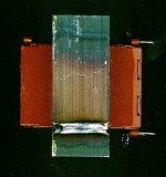
Well it seems that transformers are not what they used to be. See attached the side image of one advertised as a 'clamped' 50VA transformer made by Dagnall Electronics.
All the 'E's are together, and all the 'I's are together, and they look as if they have been 'clamped' prior to being run welded together. This is a very hard metal join, and it goes against what I was informed as being an electrically efficient method of construction. It takes much effort to hacksaw the 'I's off the 'E's, but I am continuing with this as part of an initial test bed for my 50W bipolar prototype valuation with three transistors per half; a six per half 100W version is already penned.
Hi Susan,
I have four 400VA 7kg 56V 7A 30-35 year old E-I mains transformers in the shed. ( they make a useful isolating/110V transformer ) The external metal dimensions are 5.25 wide, 4.375 high and 2.25 inches thick, with possibly 116 - 0.5mm laminations.
Is there anywhere I can find out about their likely characteristics; the 240V 50Hz primary inductance is circa 320mH on my multimeter, and if rewound as an output transformer, what would you estimate to be the practical low frequency response at 100W - 8 ohms? Turns per volt not yet known.
Cheers ........... Graham.
Above I suggested buying stock mains transformers to self assemble alternative ratios.
Well it seems that transformers are not what they used to be. See attached the side image of one advertised as a 'clamped' 50VA transformer made by Dagnall Electronics.
All the 'E's are together, and all the 'I's are together, and they look as if they have been 'clamped' prior to being run welded together. This is a very hard metal join, and it goes against what I was informed as being an electrically efficient method of construction. It takes much effort to hacksaw the 'I's off the 'E's, but I am continuing with this as part of an initial test bed for my 50W bipolar prototype valuation with three transistors per half; a six per half 100W version is already penned.
Hi Susan,
I have four 400VA 7kg 56V 7A 30-35 year old E-I mains transformers in the shed. ( they make a useful isolating/110V transformer ) The external metal dimensions are 5.25 wide, 4.375 high and 2.25 inches thick, with possibly 116 - 0.5mm laminations.
Is there anywhere I can find out about their likely characteristics; the 240V 50Hz primary inductance is circa 320mH on my multimeter, and if rewound as an output transformer, what would you estimate to be the practical low frequency response at 100W - 8 ohms? Turns per volt not yet known.
Cheers ........... Graham.
Attachments
Hi Graham,
I think these are EI 1-3/4 Laminations. I.e. the next size up from my Zeus75 transformers.
Modern M6 silicon grain orientated steel laminations are typically 0.35 mm thick, and standard M19 steel lams are c. 0.5 mm.
However for a transformer of that age I can't really tell as steel grades can vary quite a lot (and have improved).
You should be getting down towards 25 Hz for this size, and maybe better.
When you strip the transformer the tongue should be 1-3/4" wide and the gaps and outer pieces should be 7/8".
If the steel is not M6 then the bandwidth and distortion characteristics won't be as good as with M6, but the transformer will work. If you then need some I can get you M6 laminations.
For my amps I work on the basis of about 4 turns per power supply DC volt.
I.e. I run about 32-34 volts supply, and for the quad filar single chamber bobbin I get between 120 (hand wound) to 140 turns (machine wound) per wire.
For the 1-3/4" lamination size transformer you will get a few more turns if you use 1.0mm wire. If you used thicker than 1.0 mm wire you could tri-filar wind if you only want a 2:1 step down (as I normally use two of the windings in parallel for the output winding in smaller wire diameters).
Best wishes,
Susan.
Graham Maynard said:Hi Susan,
I have four 400VA 7kg 56V 7A 30-35 year old E-I mains transformers in the shed. ( they make a useful isolating/110V transformer ) The external metal dimensions are 5.25 wide, 4.375 high and 2.25 inches thick, with possibly 116 - 0.5mm laminations.
I think these are EI 1-3/4 Laminations. I.e. the next size up from my Zeus75 transformers.
Is there anywhere I can find out about their likely characteristics; the 240V 50Hz primary inductance is circa 320mH on my multimeter, and if rewound as an output transformer, what would you estimate to be the practical low frequency response at 100W - 8 ohms? Turns per volt not yet known.
Modern M6 silicon grain orientated steel laminations are typically 0.35 mm thick, and standard M19 steel lams are c. 0.5 mm.
However for a transformer of that age I can't really tell as steel grades can vary quite a lot (and have improved).
You should be getting down towards 25 Hz for this size, and maybe better.
When you strip the transformer the tongue should be 1-3/4" wide and the gaps and outer pieces should be 7/8".
If the steel is not M6 then the bandwidth and distortion characteristics won't be as good as with M6, but the transformer will work. If you then need some I can get you M6 laminations.
For my amps I work on the basis of about 4 turns per power supply DC volt.
I.e. I run about 32-34 volts supply, and for the quad filar single chamber bobbin I get between 120 (hand wound) to 140 turns (machine wound) per wire.
For the 1-3/4" lamination size transformer you will get a few more turns if you use 1.0mm wire. If you used thicker than 1.0 mm wire you could tri-filar wind if you only want a 2:1 step down (as I normally use two of the windings in parallel for the output winding in smaller wire diameters).
Best wishes,
Susan.
Hi Susan,
Thanks for the info.
My first attempt is running, and the midrange is nicely liquid.
However I already conclude that the current corollary won't work because -
*it is the taking of current from the input transformer that degrades its performance*.
You are not significantly loading your input transformers because you follow them with a tube or Mosfet stage, and thus the passband does not significantly become device limited.
More thought needed here if bipolar is to be used, but that is my next step because the lack of 'loudspeaker characterisation' is very pleasing.
Cheers for now ......... Graham.
Hi Susan,
Further findings/observations.
Above I have written that your output stage operates like a class-AB.
That is close, but *not correct*.
My simulations are showing that your output stage does not actually drop out of class-A, and thus there is never any 'crossover'.
This, with fractional output transformer resistance (impedance) and no propagation delayed global NFB, means that a dynamic loudspeaker cannot cause the output devices to reverse commutate through any portion of their fixed bias potential, as can happen in a conventional amplifier before the delayed NFB establishes accurate output potential correction.
The 'follower' output halves can be biased to behave near exponentially, and thus operate optimally in an approximate 'difference of two squares' or 'd2s' push-pull arrangement.
Your biasing is but a fraction of the current requirement for conventional class-A quality reproduction.
This situation arises because the bias potential and the local voltage feedback encompass both the output device and the load on a per-half basis.
Where the bias and feedback are derived prior to the load, as with 'conventional' solid state amplifiers, then the output devices cannot maintain on-going conduction unless operated in class-A.
Thus the 'follower' output stage can run in class-A with as little as 100mA of quiescent output bias, but the transconductance characteristics might then not be sufficiently well matched for optimal 'd2s' operation.
The output transformer is an essential part of this, for distortion and error correction arising in one output half cannot jointly interfere with input drive to the other, nor can it coincidentally interact at a co-connected output biasing network, as does happen with 'conventional' global NFB/ differential input amplifier circuitry !!!!!
(This can also happen in complementary class-A amplifiers, though not with the JLH.)
My first bipolar amplifier had too low an input impedance with parallel bias circuitry and feedback shunting the input transformer (the current corollary), and thus the transformer was over-loaded at lf and hf. However, the mid range was clean, and reproduction sounded as if the output from each push-pull half was properly 'melting' in with that of its partner, which made me think about the distinctiveness of distortion that intrudes upon our experience in 'conventional' NFB amplifiers, with their tiny high frequency 'per-half' differences.
My next test circuit is having the input transformer in series with input base bias, also with the series feedback at the first emitters wrt the output transformer centre-tap (as per your Mosfets). I shall also have 'follower' driver and output devices on a 'per-half' basis bootstrapping the input transistor, with a quiescent current of about 250mA per half to approximate 'd2s' operation.
Over the next few days I am hoping to hear not just 'liquid' mid range, but all of the bass and treble 'melting' together; the audio equivalent of chocolate ?
Susan. Over the decades I have constructed on baking tins; bird's nest wired up some low power circuits; 'pcb'ed on cardboard/stripboard, and bread boarded on lengths of 6 by 1; but my oh my, your actual real-life breadboards really do look smart supporting those 6C33Cs. (Follower bootstrapping might further reduce their distortion.)
Cheers for now ......... Graham.
Graham Maynard said:Hi Susan,
Further findings/observations.
Above I have written that your output stage operates like a class-AB.
That is close, but *not correct*.
My simulations are showing that your output stage does not actually drop out of class-A, and thus there is never any 'crossover'.
This, with fractional output transformer resistance (impedance) and no propagation delayed global NFB, means that a dynamic loudspeaker cannot cause the output devices to reverse commutate through any portion of their fixed bias potential, as can happen in a conventional amplifier before the delayed NFB establishes accurate output potential correction.
The 'follower' output halves can be biased to behave near exponentially, and thus operate optimally in an approximate 'difference of two squares' or 'd2s' push-pull arrangement.
Your biasing is but a fraction of the current requirement for conventional class-A quality reproduction.
This situation arises because the bias potential and the local voltage feedback encompass both the output device and the load on a per-half basis.
Where the bias and feedback are derived prior to the load, as with 'conventional' solid state amplifiers, then the output devices cannot maintain on-going conduction unless operated in class-A.
Thus the 'follower' output stage can run in class-A with as little as 100mA of quiescent output bias, but the transconductance characteristics might then not be sufficiently well matched for optimal 'd2s' operation.
Cheers for now ......... Graham.
Graham,
AFAIK this is does not appear correct. The OP stage will operate
in class AB. It has to. The OP transformer is centre tapped so
each prmary will swing equally and opposing around zero V.
Since the gate drive also swings equally around 0 V then
as one OP mosfet turns on the other will turn off.
The only way to get this circuit to stay in class A (past what it
would normally do for a given bias current) is to dynamically
control the centre tap of IP transformer secondary (Vbias).
Please explain if I have got this wrong.
Regards,
Terry
Graham Maynard said:[snip]This, with fractional output transformer resistance (impedance) and no propagation delayed global NFB, means that a dynamic loudspeaker cannot cause the output devices to reverse commutate through any portion of their fixed bias potential, as can happen in a conventional amplifier before the delayed NFB establishes accurate output potential correction.[snip]
This is incorrect. The reverse commutation, if any, by the loudspeaker is necessarily limited in freq by the velocity of the coil/cone. That limits it to audio frequencies. The so-called 'delayed nfb' is, in comparison, infinitely faster with delays in fractions of uSec if not nSecs. From the practical point of view of the reverse commutation, the nfb reacts instantly.
Jan Didden
Here http://vlauga.narod.ru/FS.htm how to make stepup the transformer for the transistor amplifier, more than high-quality (at presence of qualitative mu-iron) and rather simple in manufacturing.
And here http://astral-for.narod.ru/index/stones/amgen.gif
The amplifier where such transformer is applied, zero feedback, K amp_U semiconductor cascad = 1, Pout = (Uin*Ktr) ^2/Rspk
Unfortunately, while all in Russian.
And here http://astral-for.narod.ru/index/stones/amgen.gif
The amplifier where such transformer is applied, zero feedback, K amp_U semiconductor cascad = 1, Pout = (Uin*Ktr) ^2/Rspk
Unfortunately, while all in Russian.
Terry Demol said:Graham,
AFAIK this is does not appear correct. The OP stage will operate
in class AB. It has to. The OP transformer is centre tapped so
each prmary will swing equally and opposing around zero V.
Since the gate drive also swings equally around 0 V then
as one OP mosfet turns on the other will turn off.
No, he is correct. Remember, it's a follower circuit. As a gate starts to go less positive, the source also goes less positive. The AC signal between any given gate-source pair is (almost) zero... Also, as an aside, gate voltage swings around a positive bias voltage of about 2-4 volts depending on the MOSFETs used and bias current desired.
Peace
Hi Terry,
I have picked a Mosfet at random. See illustration.
Often the increase in current with increasing voltage is greater then the decrease with an equal but opposite amplitude variation..
As you say both inputs are equal and opposite, and the more conducting half drives the other oppositely, but that does not mean that the more inactive device becomes cut off prior to overloading non-linearity, which is non-latching and without additional reactive NFB loop generated error.
I have simulated bipolar circuits similarly. They can be made to not cut off, or be allowed to do so.
*Thanks Roscoe.
Hi Jan,
If I take time to argue this point I will use up what precious time/health I have available to me for making progress.
I cite 'conventional' amplifier; ie. diff+VAS+driver+out with compensation.
Crossovers and cabinets can generate substantial back EMFs that are not directly related to on-going signal, and which can cause amplifier non-linearity and thus degraded NFB loop correction. The amplifier is obliged to react and does so correctly only for the time that it can operate linearly.
NFB might act practically instantly, but that does not necessarily mean that it will accurately *correct* in fractions of a uS within most amplifiers, and it does not take much for additional error to be generated.
Cheers for now ......... Graham.
Attachments

Graham: what's the bias current in your simulation? What will happen if you dial it back to like 100ma?
Putting aside this back EMF thing that no one understands, what will happen to the upper mosfet during the negative cycle of a sine signal?
Susan's circuitry is simple to understand, and has been well understood for decades, as class AB. Why make it more complicated than it really is?
Putting aside this back EMF thing that no one understands, what will happen to the upper mosfet during the negative cycle of a sine signal?
Susan's circuitry is simple to understand, and has been well understood for decades, as class AB. Why make it more complicated than it really is?
Hi tlf9999,
Had I though more before entering my own findings/observations to this thread that challenges/comments not directly related to Susan's work might arise, then I would not have done so.
Yes, Susan's circuitry is delightfully simple, and thus it is also extremely easy to simulate.
Don't forget that a follower output stage does not run a 'negative' cycle wrt a fixed plus commoned quiescent bias in the same way that normally illustrated common cathode/emitter/source, transformerless or complementary push-pull circuits do wrt a fixed supply rail.
Also don't forget that optimum biasing arises when the device with reducing output conduction contributes to output that which is lost by stage inefficiency in the main conducting half.
Mosfets/tubes run in classes A/AB1(2)/B when the output arises at the drain/anode wrt source/cathode; this is not the same as when balanced output arises at the source/cathode wrt drain/anode, and it is likely that we did not see more of this type of design decades ago due to the challenge of reliable heater-cathode insulation and the already acceptable triode amplification.
In a 'source follower' output stage, equal but opposite voltages develop at the *sources* wrt drain; thus, the lesser conducting half normally reqires a greater than equal but opposite negative input voltage wrt bias (than the positive input voltage generates the output) for it to fully drop out of conduction; as per the non linear Mosfet characteristics I illustrated above. With normal devices the greater the output voltage, the lower the relative gate voltage would need to be wrt equal bias for the less conducting device to drop out of class-A operation.
My original thoughts about this circuit were insufficiently founded; thus I re-clarified. With normal devices the longer and gradual low level transconduction characteristics mean that with properly wound input/output transformers neither of the output devices drops out of shared conduction until output load demands upon the conducting device exceed its natural capability.
Cheers ............ Graham.
Graham Maynard said:With normal devices the longer and gradual low level transconduction characteristics mean that with properly wound input/output transformers neither of the output devices drops out of shared conduction until output load demands upon the conducting device exceed its natural capability.
Cheers ............ Graham.
I thought that's exactly how class B (or AB as some may prefer) is defined, albeit in a more easily understood way. another way to put it, a Class B (or AB) amp works in Class A when it is not working in Class B, 🙂.
tlf9999 said:
I thought that's exactly how class B (or AB as some may prefer) is defined, albeit in a more easily understood way. another way to put it, a Class B (or AB) amp works in Class A when it is not working in Class B, 🙂.
No, it's not. In a class B amp, BOTH devices are in (or nearly in) cutoff with no signal applied. In a class AB amp, it takes a larger signal to cause one device to cut off for part of the signal, but this happens at signal levels considered as within the normal operating range of the amplifier. In a class A amp, neither device will ever be in cutoff under normal operating conditions (any class A amp will start to look like a class AB amp if you overdrive it hard enough). Susan's design, in this reguard, operates like a class A amp, neither device will be in cutoff until the amp is trying to swing more votage than the power supply rail will allow it to swing.
Peace
Hi Graham,
Thank you very much for your further thoughts and taking time to reply to questions arising form them 🙂
Ah chocolate, yes I can relate to that analogy 🙂
Thank you.
Best wishes,
Susan.
Graham Maynard said:Hi Susan,
Further findings/observations...
Thank you very much for your further thoughts and taking time to reply to questions arising form them 🙂
Over the next few days I am hoping to hear not just 'liquid' mid range, but all of the bass and treble 'melting' together; the audio equivalent of chocolate ?
Ah chocolate, yes I can relate to that analogy 🙂
Over the decades I have constructed on baking tins; bird's nest wired up some low power circuits; 'pcb'ed on cardboard/stripboard, and bread boarded on lengths of 6 by 1; but my oh my, your actual real-life breadboards really do look smart supporting those 6C33Cs.
Thank you.
Best wishes,
Susan.
Peace or Graham: since the circuit is so easy to simulate, maybe you can show the current going through the upper MOSFET assuming the following:
a) rail of 40vdc;
b) bias of 100ma;
c) driven by a 30vpp sine signal at the gate of the MOSFET.
Will the upper MOSFET shut off during at least part of the cycle?
a) rail of 40vdc;
b) bias of 100ma;
c) driven by a 30vpp sine signal at the gate of the MOSFET.
Will the upper MOSFET shut off during at least part of the cycle?

rozak said:simulation
is this class A or class B (or AB if you prefer)?
I thought this particular topology has been thoroughly studied and used (in a slightly different variation) for decades in old transistor radios.
Sure, technology has advanced and our understanding of semiconductor physics has advanced, and more of us can spell quiescent current or push-pull or gate capacitance or back EMF without understanding any of them but does that really change the way this circuit works?
- Home
- Amplifiers
- Solid State
- Zero Feedback Impedance Amplifiers