The loopgain simulation was done almost the same way that Preamp has described.
The trace is labeled 'V(n002)', that's why I assumed it was a closed loop measurement.
You seem to have made a mistake here, at the start.
The definitions in your quoted links are essentially (to avoid clumsy pedantry about PNP or NPN polarities) that Vbc becomes forward biased. This is the formal definition that I learned too, for BJT.
That is not the same as Vce=0, yes?
Once and for ever. Vce=0 is a limit case that is not encountered in practice, at least not in analog electronics. Get a npn, tie the base to the collector, apply a voltage Vcc>0 between the collector and the emitter. The npn transistor is at what is called "incipient saturation", Vcb=0 and Vce=Vbe.
Now tie the collector to Vcc>0 and the base to Vdd > Vcc The npn transistor is now "saturated" and as soon as Vdd approaches Vcc + 0.7V, and hence Vce->0, this is "hard saturation". Note that the BC junction is forward biased in this case.
At "incipient saturation", as jcx mentioned, the transistor has still enough beta to work, although most of the usual device models are failing. That's how micropower opamps working at 1V are designed, here's an example.
Last edited:
I posted the definition verbatim.
You copy/pasted the definition from www.whatis.com That's barely what I would call a reliable source.
I posted the definition verbatim...
Simply a case of different definitions.
The definition that Waly linked is clear cut and thus useful for education and formal papers.
Yours is an operational definition and useful in practice.
Probably also more consistent with the use of the term for more than just BJTs?
Best wishes
David
Last edited:
Once and for ever. Vce=0 is a limit case that is not encountered in practice...
Exactly. You were the one who said "... saturation is at Vce=0". [1]
I don't understand why you try to defend this when it is not correct, the "yes?" at the end of my post was only a rhetorical invitation for you to admit that it was just a typo.
Best wishes
David
[1] In post #280.
Last edited:
That is my TT amp you are talking about, there is protection resistor between EF collector and the ground and that EF never blew. It was my first blameless that blew.
I simulated exactly your connection of the current limiting transistor and that simulation shows that EF transistor is going to blow before the current limiter even start to limit. That shows that is not important where the current limiting transistor is connected, without that resistor EF will blow at heavy overload.
Well, you've been shown where you went wrong, but you still seem to want to argue about it. My version has been keeping VAS transistors intact for at least twenty years, in mass-production for four different manufacturers. This adds up to tens of thousands of units. I call that a proven circuit.
ps. In my opinion there is no need for VAS current limiting transistor, but EF protection resistor is enough. The current limiting is needed for simple VAS with no EF enhancement.
Wrong. Be kind to your VAS transistor.
I think our work on this topic is done.
Simply a case of different definitions.
The definition that Waly linked is clear cut and thus useful for education and formal papers.
Yours is an operational definition and useful in practice.
Probably also more consistent with the use of the term for more than just BJTs?
Best wishes
David
Yes I think so, it is similar (but not identical) for a JFET where saturation current is defined as the current where increase in VDS does not lead to higher Id.
If you follow 'saturation is when increasing Ib doesn't lead to increasing Ic' you get to 'forward-biased b-c junction'. The larger this 'saturation Ib' the lower Vce becomes, anything between 0.7V and 0.05V (my experience; don't know if it can go any lower).
jan
Well Mr. Self, yes, this is a can of worms. Indeed TMC (or "output inclusive" as you call it) is a 2 pole compensation method. This was discussed here in extenso, and lots of valid theoretical reasoning was provided.
Well, the lid's off now. I am well aware that output-inclusive compensation (or TMC as it is sometimes called on this board) and 2-pole compensation were debated up hill and down dale over hundreds of pages.
I have not read them all, or more than a small minority; the section on 2-pole compensation in APAD6 was written pretty much in vacuo, with no reference to the DIYaudio debate.
To me, the most conclusive proof was the mathematical equivalence of the "output inclusive" schema with a regular 2 pole compensation network, plus a lead-lag compensation network. This is relatively easy to prove using a Wye-Delta transformation of the "output inclusive" network. The physical interpretation of this equivalence is a 2 pole compensation loop gain/phase shape, and a lead lag compensation that removes the phase dip before the unity loop gain frequency, which creates the illusion that "output inclusive" compensation is "single pole".
I don't follow this. Where does the lead lag compensation come from? Does it in some way always automatically suppress the gain-peaking you get with 2 pole compensation?
If you can give us a clear and concise explanation of this whole business, you would be doing us a great service.
The bottom of this is that much care has to be taken in using "output inclusive" compensation. Enough phase margin in the global feedback loop doesn't guarantee good stability, since the inner (or minor) feedback loop can be dangerously close to the stability limit.
This is absolutely not my experience. Inclusive amplifiers (Blameless + output-inclusive compensation) are just as stable as ordinary dominant-pole versions. As described in Chapter 12 of APAD6, stability was checked with reactive loads and 4-Ohm loads, the latter being the more severe test due to the changed conditions in the output stage.
I find output-inclusive compensation a beautifully tractable and highly effective enhancement, and I really, really wish I had invented it.
I know these things can be rather slippery, and may raise more questions that they answer, so before going into any details, I must ask what would you consider as valid proof that "output inclusive" is 2 pole compensation method. BTW, it took Mr. Cordell about six months to buy into this, now he fully agrees with this "2 pole" view of TMC/"output inclusive".
Just a clear explanation would do. I'm sure all the information already exists in the board debates, but winnowing through them would be a daunting task for someone not familiar with the material, which I assume you are.
Last edited:
Exactly. You were the one who said "... saturation is at Vce=0". [1]
It's not correct, I assume it was just a typo, I don't understand why you try to defend it.
Best wishes
David
[1] In post #280.
Please quote me correctly and add "...in analog electronics". In switching circuitry Vce->0 is pretty common, to minimize forward conduction losses.
Vce=0 is the standard definition of "hard saturation", since this the only saturation regime where the device gain vanishes. As I already mentioned, "incipient saturation" is not "true" saturation, since the device still has gain.
I would concede though that Vce=0 is a rather conventional/theoretical value, since the built in potentials of the Vbe and Vcb junctions are different. It would be more realistic to put something like Vce=50mV, but then the value would depend on device type, size and process.
Yes Horowitz & Hill say something similar (H & H, Appendix G):
'In switching apps you provide generous amounts of base current (typically 1/10 to 1/20 of Ic) to achieve Vce(sat) of 50mV to 200mV.'
You do this to avoid the off-chance that the switch gets out of saturation when Ic required goes up for any reason.
In analog use they agree that saturation is reached when the b-c diode starts conducting.
So they also see a difference between 'hard' and 'soft' saturation.
I must concede this is a bit hazy for me since the last time I worked with saturated switches was in 1964 (yes!) helping Philips to develop a full transistor b/w TV, using a germanium AU103 (800V TO-3) as line switch at 15,625 Hz. Except we didn't call it 'saturation' but 'bottoming'.
Jan
Last edited:
Please quote me correctly...
I did quote you correctly. I did not quote you completely because we are both in accord about the omitted material.
Vce=0 is the standard definition of "hard saturation"...
Had you written "Hard saturation is ..." then you would have a perfect point, but the 3 definitions that you yourself posted [1] are consistent and they all define "saturation" as Vce less than Vbe, not as Vce=0.
And that's what you wrote, I could quote it correctly for the third time but I have better work to do.
Best wishes
David
[1] Post #304
Last edited:
if you want to come to an understanding shared by Bob Cordell, Dave Zan as fellow authors papers on audio amp theory...
(assuming you are dismissing the rest of merely competent EEs on this site such as Syn08, megajocke, that have put up substantive analysis here or on other websites, and a larger number of others that have followed, made intelligent comments on the discussion)
try understanding these 2 pics that are sim plots comparing dominant pole Miller and TMC/OIC with the same loop stability "challenge"
stepped increasing delay added to the output stage, inside the loop(s) - the cleanest illustration/test of "phase margin" I could come up with
the responses are very different when the compensation is the only change - even though the gain probe test source is just cutting the outer global feedback loop in both plots
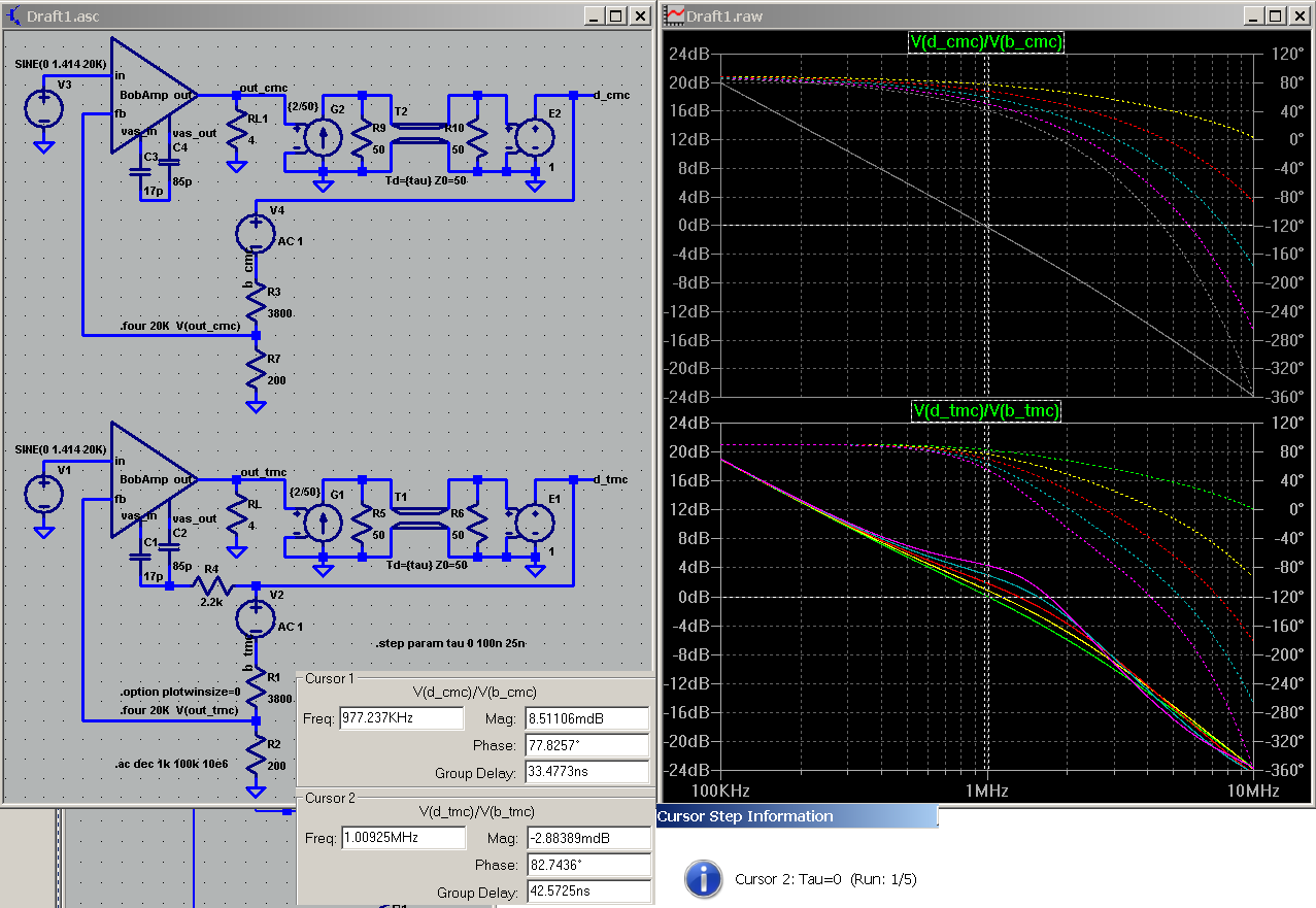
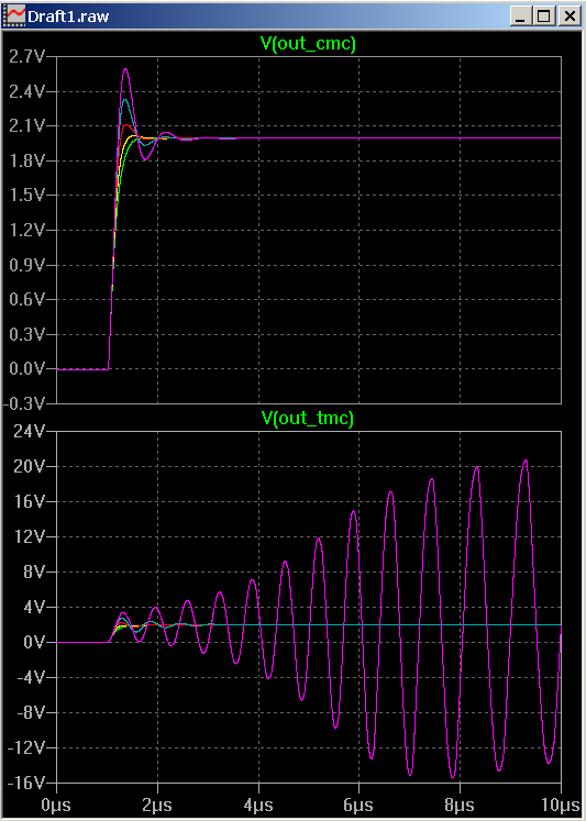
TMC/OIC is not "as safe" as Miller dominant pole compensation - it has to be designed to the same standards as 2-pole compensation
the links to my attempt to clarify, educate have have been pointed out to you a few times now http://www.diyaudio.com/forums/soli...-6th-edition-douglas-self-28.html#post4014173
(assuming you are dismissing the rest of merely competent EEs on this site such as Syn08, megajocke, that have put up substantive analysis here or on other websites, and a larger number of others that have followed, made intelligent comments on the discussion)
try understanding these 2 pics that are sim plots comparing dominant pole Miller and TMC/OIC with the same loop stability "challenge"
stepped increasing delay added to the output stage, inside the loop(s) - the cleanest illustration/test of "phase margin" I could come up with
the responses are very different when the compensation is the only change - even though the gain probe test source is just cutting the outer global feedback loop in both plots
TMC/OIC is not "as safe" as Miller dominant pole compensation - it has to be designed to the same standards as 2-pole compensation
the links to my attempt to clarify, educate have have been pointed out to you a few times now http://www.diyaudio.com/forums/soli...-6th-edition-douglas-self-28.html#post4014173
and of course simplest of all is just take the suggestion to put the loop gain probe inside all loops, cutting between the output Q and both the inner loop "bootstrap" R and global feedback parts
Last edited:
The distinction between Vce=0 and Vcb < Vbe is one that you made and about which you criticised other people's comprehension.
Bit rich to call it a quibble once you turn out to be incorrect😉
Best wishes and bye for now
David
Bit rich to call it a quibble once you turn out to be incorrect😉
Best wishes and bye for now
David
...shared by Bob Cordell, Dave Zan as fellow authors papers on audio amp theory...
OK, I planned to stay out of this until I had a 6th edition handy to update my 5th, but I can't resist😉
Your delay simulations are excellent, but what I found educational was to do a star delta transform of TMC and see it turn into TPC.
I think you had already proposed this before I did it, but luckily I was unaware, because to work it out for oneself is informative in a way that other people's examples usually don't match.
Just one point, I see mention of "output inclusive" compensation.
I think it is important to separate TMC, clearly a two pole (and one zero!) system, from "output inclusive" that can be just one effective pole.
Perhaps this is the cause of some misapprehensions, I am not sure how the term has been used.
Best wishes
David
Last edited:
waly I think has the local/proximate web TMC analysis history straight(er) http://www.diyaudio.com/forums/soli...one-seen-front-end-before-35.html#post3037995
I would have 1st seen, and then did duplicate for myself in Mathcad Syn08 Popa Ovidiu analysis on the now dead site
I would have 1st seen, and then did duplicate for myself in Mathcad Syn08 Popa Ovidiu analysis on the now dead site
I think you had already proposed this before I did it, but luckily I was unaware, because to work it out for oneself is informative in a way that other people's examples usually don't match.
Syn08 originally did it and posted it on the now defunct dyaudio-engineering.org where we all were members (me, late, soon before closing down).
if you want to come to an understanding shared by Bob Cordell, Dave Zan as fellow authors papers on audio amp theory...
(assuming you are dismissing the rest of merely competent EEs on this site such as Syn08, megajocke, that have put up substantive analysis here or on other websites, and a larger number of others that have followed, made intelligent comments on the discussion)
I'm not dismissing anything or anybody.
try understanding these 2 pics that are sim plots comparing dominant pole Miller and TMC/OIC with the same loop stability "challenge" stepped increasing delay added to the output stage, inside the loop(s) - the cleanest illustration/test of "phase margin" I could come up with. The responses are very different when the compensation is the only change - even though the gain probe test source is just cutting the outer global feedback loop in both plots
I think I see what you mean- the added delay with OIC causes peaking in the gain plot, (I assume that is the straight line in the upper plot) which makes sense. However it does not look anything like the gain peaking you get with two-pole compen, in which the gain continues flat to a much higher frequency, does a little peak and then falls at 12 dB/octave. (See p343 of APAD6)
Many thanks for posting that example.
TMC/OIC is not "as safe" as Miller dominant pole compensation -
As I said, this is not my experience in dealing with real amplifiers. The majority of designs in APAD6 had OIC just slapped onto them, same component values each time, without a hint of trouble, which was very satisfying. Reactive and 4-Ohm loads were tried; no problems. See Chapter 12 of APAD6.
it has to be designed to the same standards as 2-pole compensation
In what ways, specifically?
the links to my attempt to clarify, educate have have been pointed out to you a few times now http://www.diyaudio.com/forums/soli...-6th-edition-douglas-self-28.html#post4014173
Well, I'm always ready to learn, but I can't tackle everything at once.
Last edited:
I don't follow this. Where does the lead lag compensation come from? Does it in some way always automatically suppress the gain-peaking you get with 2 pole compensation?.
Mr. Self, it is very, very hard to explain this without making use of lots of algebra, and this forum is not formulae friendly. Anyway, here's the basic plot.
Draw the VAS as a gain stage of transconductance -Gm and load Z (which, in this case, you may assume is resistive) and the output stage as an ideal voltage amplifier of gain +1. Around this configuration, draw the output inclusive compensation, as a Wye network with nodes at the VAS input, at the VAS output and at the amplifier output. The Wye elements are (in the same order) 1/jwC1, 1/jwC2 and R (of the output inclusive network) where C2>>C1.
A Wye-Delta transformation defines the values of the Delta network (having the corners in the Wye network nodes) as a function of the Wye network elements, see this. It is guaranteed that the Delta equivalent network does not change either the branch currents or the node potentials in the circuit.
Now, if you draw the Delta equivalent elements and calculate their impedances, you will get after much algebraic blood sweet and tears (and certain simplifications, like ignoring the additional output impedance , since its real and imaginary parts are much higher than the output impedance, etc...) you'll get the standard 2 pole compensation network, plus an RC series group, connected between the VAS input and the amp output. That's the lead lag compensation, and yes indeed, you got it right, this lead lag network "automatically suppresses the gain-peaking you get with 2 pole compensation".
If you need all the math details, you may want to contact syn08 (the author of this beautiful equivalence proof), I'm sure he has them in electronic format (I can't post my paper scribbles). It's the PGP website owner you already looked at, and his email is on the web site. The beauty of this method is that, given the 2 pole compensation network elements, the equivalent (in the sense of providing exactly (within a few %) the same unity loop gain frequency and phase margin) output inclusive compensation network can be calculated. And the other way around, of course, from TMC to a 2 pole + lead lag network.
Sorry, this is all I can help with.
P.S. AndyC, if by chance you are reading this, *please* reopen that forum, at least for read only. I see you still own the domain.
Last edited:
- Status
- Not open for further replies.
- Home
- Amplifiers
- Solid State
- Your opinions are sought on Audio Power Amplifier Design: 6th Edition. Douglas Self