Thanks. I'll keep an eye on this one to see how the outputs behave. Unfortunately I don't have the test equipment to see if the distortion levels are in spec.
It does seem odd that the output board was inoperative. First one I have seen like this. That said, there was only the blown driver transistor. The actual TO3 output devices were all OK.
So I guess we will see.
I have the new adjustable current source chip at home (I am traveling this week), so I'll try out the breadboard current source this weekend. The idea of this is really just that both the positive and negative current sources are referenced to voltage references that derive from exactly the same current source. So, to the degree that the resistors in that reference leg are the same, the currents in the diff pairs will be the same. Getting precision resistors is easy. I am just not certain that I can get a match down at the level I need.
In the original we have two LEDs that may or may not be driven at the same current level, so there is one offset source, and then we have the actual current sources that derive from those. So, several sources of potential imbalance. I'll experiment with some tuning pots, but I hope they will not be necessary.
Basically, if I aim for a max offset of 1 volt at the output without the servo, then that translates to diff pair load resistor voltage drop match of about 10 mV, which is a current match of 10 uA. This also implies that without any other adjustments, the diff pairs need to be a matched set of FOUR...so not just matched pairs, but pairs of matched pairs.. to the extent that this is not the case, the servo will have to correct it. The reason for this is that if the currents in the diff pairs are not equal, then the currents in the load resistors (R106 and R107) will not be equal, and there will be an offset.
I totally agree that the servo is sort of an afterthought...
I tested the soft start relay, using a power supply, and it seems to work. I think maybe the relay somehow got stuck off, but it seems to be working now. I replaced the 20 watt resistor, and put it all back together.
The soft start board works fine now, and the amp comes up perfectly. Looks like the output is swinging about +/- 75 volts peak at clipping, which is about 350 watts RMS.
Time to button this one up, and start on #4. I'll pick the best three of the four, and probably give the spare to my son for his setup.
Cheers,
Scott
I also breadboarded my bi-polar current source. This is an experiment to replace and improve on the existing control board current source circuit.
Here is a brief walkthrough of the original current source circuit:

The emitter of Q119 goes through the heatsink thermal switches, and eventually goes out pin 2 of the J106 connector. this leads it to the opto coupler on the soft start board. R151 and R152 form a voltage divider that puts about 42 volts on pin 3 of J106. When the soft start board is energized, the opto-coupler closes the circuit between pins 2 and 3 of J106, thereby allowing current to flow in Q119.
When current is NOT flowing through Q119, R150 bypasses D115 (which is a 2.5 volt reference diode), so the base of Q118 is at about -85 volts and Q118 is off. With Q118 offR146 bypassed the LED D114, putting the bases of Q117, and Q1154 at about +85 volts, and this causes Q117 and Q115 to be off. With Q117 off, the same thing occurs at D113 and Q116. With Q116 and Q115 off, there is no current though the input stage diff pairs, and the amplifier will have no audio signal amplification. Since the emitter of Q119 is also connected in series with the heatsink thermal switches, any excessive heating of the amplifier will open those switches and also cut off the input stage current, thereby shutting down the amp.
When the emitter of Q119 is connected through the opto coupler to the voltage source formed by R151 and R152, then current flows through R150, placing D115 into reverse bias. Since it is basically a zenber, this sets the voltage at the base of Q118 at 2.5 volts.
With the base od Q118 at 2.5 volts, the voltage at the emitter is also fixed (at about 1.9 volts), and this creates a constant current flow across the emitter collector junction of Q118. This current is sourced through R146 and D114, thereby creating a fixed voltage at the base of Q117 and Q115.
With a fixed voltage at the base of Q115, the voltage at the emitter of Q115 is fixed, and this means that the voltage drop across R144 is fixed. the current sourced by Q115 is therefore set by the voltage drop across R144. As the load on this leg changes, the voltage at the collector of Q115 will vary to maintain the current (and the drop across R144) fixed.
The base of Q117 is tied to the base of Q115, and so Q117 operates in the same way, creating a constant current through D113 and R147, which forces the emitter of Q116 to be at a fixed voltage, thereby creating the constant current SINK for the other diff pair.
This works, but as you can see, the current for each did pair is set by the voltages at the emitters of Q115 and Q116. These voltages are related, but they are not necessarily exactly the same. If the current through Q118 is not exactly the same as the current through Q117, then the drops across D114 and D113 will be slightly different and the currents created by Q115 and Q116 will be different.
In the input amplifier, these currents flow through the diff pairs and eventually set the drop across R106 an R107 (both precision 1K resistors). This drop is what sets the bias point for the driver stages (Q110/Q112, and Q109/Q111), and to the extent that these are not perfectly matched, there will be a DC offset at the output. Normally the server then generates a small input offset to compensate for this.
This works, but it relies on the server to iron out any errors, so it is not super stable.
I initially wondered why they designed this to operate from the +/- 85 volt rails. In reality the drops across R153 and R154 put the operating rails at about +/-75 volts, but the current source actually only needs to provide about +/- 1.6 volts at the output of the current source. I think they did this to isolate the bias circuit from any variations and noise on the power supply lines. If there is a change on the positive rail, then technically the current source voltage will also change, and that will keep the drop across the load resistors (R106/107) fixed. This is not exactly true, however, since the negative supply rail provides the current sink for the positive side diff pair, so this approach only balances out common mode noise and errors (noise and supply voltage variations that occur on both rails at the same time.
I'll describe my proposed solution in the next post.
Here is a brief walkthrough of the original current source circuit:
The emitter of Q119 goes through the heatsink thermal switches, and eventually goes out pin 2 of the J106 connector. this leads it to the opto coupler on the soft start board. R151 and R152 form a voltage divider that puts about 42 volts on pin 3 of J106. When the soft start board is energized, the opto-coupler closes the circuit between pins 2 and 3 of J106, thereby allowing current to flow in Q119.
When current is NOT flowing through Q119, R150 bypasses D115 (which is a 2.5 volt reference diode), so the base of Q118 is at about -85 volts and Q118 is off. With Q118 offR146 bypassed the LED D114, putting the bases of Q117, and Q1154 at about +85 volts, and this causes Q117 and Q115 to be off. With Q117 off, the same thing occurs at D113 and Q116. With Q116 and Q115 off, there is no current though the input stage diff pairs, and the amplifier will have no audio signal amplification. Since the emitter of Q119 is also connected in series with the heatsink thermal switches, any excessive heating of the amplifier will open those switches and also cut off the input stage current, thereby shutting down the amp.
When the emitter of Q119 is connected through the opto coupler to the voltage source formed by R151 and R152, then current flows through R150, placing D115 into reverse bias. Since it is basically a zenber, this sets the voltage at the base of Q118 at 2.5 volts.
With the base od Q118 at 2.5 volts, the voltage at the emitter is also fixed (at about 1.9 volts), and this creates a constant current flow across the emitter collector junction of Q118. This current is sourced through R146 and D114, thereby creating a fixed voltage at the base of Q117 and Q115.
With a fixed voltage at the base of Q115, the voltage at the emitter of Q115 is fixed, and this means that the voltage drop across R144 is fixed. the current sourced by Q115 is therefore set by the voltage drop across R144. As the load on this leg changes, the voltage at the collector of Q115 will vary to maintain the current (and the drop across R144) fixed.
The base of Q117 is tied to the base of Q115, and so Q117 operates in the same way, creating a constant current through D113 and R147, which forces the emitter of Q116 to be at a fixed voltage, thereby creating the constant current SINK for the other diff pair.
This works, but as you can see, the current for each did pair is set by the voltages at the emitters of Q115 and Q116. These voltages are related, but they are not necessarily exactly the same. If the current through Q118 is not exactly the same as the current through Q117, then the drops across D114 and D113 will be slightly different and the currents created by Q115 and Q116 will be different.
In the input amplifier, these currents flow through the diff pairs and eventually set the drop across R106 an R107 (both precision 1K resistors). This drop is what sets the bias point for the driver stages (Q110/Q112, and Q109/Q111), and to the extent that these are not perfectly matched, there will be a DC offset at the output. Normally the server then generates a small input offset to compensate for this.
This works, but it relies on the server to iron out any errors, so it is not super stable.
I initially wondered why they designed this to operate from the +/- 85 volt rails. In reality the drops across R153 and R154 put the operating rails at about +/-75 volts, but the current source actually only needs to provide about +/- 1.6 volts at the output of the current source. I think they did this to isolate the bias circuit from any variations and noise on the power supply lines. If there is a change on the positive rail, then technically the current source voltage will also change, and that will keep the drop across the load resistors (R106/107) fixed. This is not exactly true, however, since the negative supply rail provides the current sink for the positive side diff pair, so this approach only balances out common mode noise and errors (noise and supply voltage variations that occur on both rails at the same time.
I'll describe my proposed solution in the next post.
As I noted above, the original current source was powered from the +/- 85 volt rails. I may try to work out a scheme for doing that, but my current approach is actually to run the current sources off the +/-14 volt regulators used for the input stage active load (cascode) bias and the servo. I may decide this is not a good idea, but for now I think it is a better approach.
Here is the circuit.

Other than some value differences, the output stages of the current sources are the same. The loads R6 and R7 represent the diff pair loads, and are not part of the circuit as it would be implemented in the amp.
The key difference in the rest of the circuit is that I have derived the base voltages (and thus the emitter voltages) for Q115 and Q116 from a single source.
I am using an LM 234 constant current source. This device generates a constant current which is set by the resistance between pins 2 and 3 (R5 and R12 in the diagram). R4 is there to provide thermal compensation (as recommended by the maker).
This setup means that the current through the entire chain R3, LED 1, LED2 and R9 is the same. So, to the degree that the resistor pairs R9 and R3, and R2 and R2, and LEDs are matched, the voltage drop across R1 will be the same as the drop across R2, and the currents created by Q115 and Q116 will be the same.
When the resistance between pins 2 and 3 on the LM234 device is large, the current flow drops to about 2 micro amps. You can see that I have used another opto-coupler as a solid state relay in that part of the circuit. This replaces the control function provided by Q119 in the original circuit. So when the soft start board is inactive, the opto-coupler resistance is effectively infinite, and LM234 is off. This shuts down the current sources formed by Q115 and Q116, thereby turning off the input stage of the amplifier. When the Soft Start board is activated, the opto-coupler resistance drops to about 22 ohms, which is much smaller than the 1K resistance that sets the current, and the current source starts working, thus activating Q115 and Q116.
With these values, the currents through Q115 and Q116 can be adjusted between about 1 mA and 6 mA.
Using regular 5% resistors, the voltage drops across the load resistors (R6 and R7) in the two legs are the same for all set point values (1 to 6 mA) within a few millivolts (which corresponds to a current match in the micro-amp range).
Interestingly, the currents do not change at all as the DC supply voltages change (within reason, of course).
What I have seen in these amplifiers is that the basic operating point gets set by the nominal (zero signal) bias point formed by the currents in the diff pairs (i.e the currents provided by this current source). To the extent that this is incorrect, the amplifier will either clip at too low a signal level (because the drivers are biased on too far), or it will simply not produce any voltage gain in the drivers (because they are biased off). IN the extreme case, where both sides are biased on too high, the output starts to operate in Class A, and the current levels are super high, the transformer buzzes, heat pours off the heatsinks, and the lights in my garage dim...
To the extent that these currents are not the same, these effects will show up unequally in the positive and negative sides of the amp. So, for example if one side is biased on more than the other, that side will clip first at high signal levels. What is not quite as apparent though is that in that situation (with no server connected) the output DC level will be offset in the direction corresponding to the driver that is biased on more heavily.
In a nutshell then, the overall signal gain (and thus output power) of the amplifier is set by the overall bias point of the diff pairs, and the DC offset (without the servo) is set by the DIFFERENCE between these current sources.
I have not shown it in the diagram above, but I also plan to include trimmers on R1 and R2, so I can fine tune this balance. This will compensate for any component value mismatches. I am assuming that thermal variations will be the same for all of the components (within reasonable levels anyway), so once any fixed errors are tuned out, the circuit should provide a solid bias point for the input stages. I'll still use the servo, but I am assuming it will be barely doing any work, and real is only there to balance out any drift that creates imbalances in the system.
I am currently working on including this approach in my re-design/re-layout of the control board. This is also interesting, since in the original a large portion of one side of the board was dedicated to this circuit, and the new one is a) much simpler, and b) located over on the input side of the board.. As a result, the overall board layout will be somewhat different.
Cheers,
Scott
Here is the circuit.
Other than some value differences, the output stages of the current sources are the same. The loads R6 and R7 represent the diff pair loads, and are not part of the circuit as it would be implemented in the amp.
The key difference in the rest of the circuit is that I have derived the base voltages (and thus the emitter voltages) for Q115 and Q116 from a single source.
I am using an LM 234 constant current source. This device generates a constant current which is set by the resistance between pins 2 and 3 (R5 and R12 in the diagram). R4 is there to provide thermal compensation (as recommended by the maker).
This setup means that the current through the entire chain R3, LED 1, LED2 and R9 is the same. So, to the degree that the resistor pairs R9 and R3, and R2 and R2, and LEDs are matched, the voltage drop across R1 will be the same as the drop across R2, and the currents created by Q115 and Q116 will be the same.
When the resistance between pins 2 and 3 on the LM234 device is large, the current flow drops to about 2 micro amps. You can see that I have used another opto-coupler as a solid state relay in that part of the circuit. This replaces the control function provided by Q119 in the original circuit. So when the soft start board is inactive, the opto-coupler resistance is effectively infinite, and LM234 is off. This shuts down the current sources formed by Q115 and Q116, thereby turning off the input stage of the amplifier. When the Soft Start board is activated, the opto-coupler resistance drops to about 22 ohms, which is much smaller than the 1K resistance that sets the current, and the current source starts working, thus activating Q115 and Q116.
With these values, the currents through Q115 and Q116 can be adjusted between about 1 mA and 6 mA.
Using regular 5% resistors, the voltage drops across the load resistors (R6 and R7) in the two legs are the same for all set point values (1 to 6 mA) within a few millivolts (which corresponds to a current match in the micro-amp range).
Interestingly, the currents do not change at all as the DC supply voltages change (within reason, of course).
What I have seen in these amplifiers is that the basic operating point gets set by the nominal (zero signal) bias point formed by the currents in the diff pairs (i.e the currents provided by this current source). To the extent that this is incorrect, the amplifier will either clip at too low a signal level (because the drivers are biased on too far), or it will simply not produce any voltage gain in the drivers (because they are biased off). IN the extreme case, where both sides are biased on too high, the output starts to operate in Class A, and the current levels are super high, the transformer buzzes, heat pours off the heatsinks, and the lights in my garage dim...
To the extent that these currents are not the same, these effects will show up unequally in the positive and negative sides of the amp. So, for example if one side is biased on more than the other, that side will clip first at high signal levels. What is not quite as apparent though is that in that situation (with no server connected) the output DC level will be offset in the direction corresponding to the driver that is biased on more heavily.
In a nutshell then, the overall signal gain (and thus output power) of the amplifier is set by the overall bias point of the diff pairs, and the DC offset (without the servo) is set by the DIFFERENCE between these current sources.
I have not shown it in the diagram above, but I also plan to include trimmers on R1 and R2, so I can fine tune this balance. This will compensate for any component value mismatches. I am assuming that thermal variations will be the same for all of the components (within reasonable levels anyway), so once any fixed errors are tuned out, the circuit should provide a solid bias point for the input stages. I'll still use the servo, but I am assuming it will be barely doing any work, and real is only there to balance out any drift that creates imbalances in the system.
I am currently working on including this approach in my re-design/re-layout of the control board. This is also interesting, since in the original a large portion of one side of the board was dedicated to this circuit, and the new one is a) much simpler, and b) located over on the input side of the board.. As a result, the overall board layout will be somewhat different.
Cheers,
Scott
I've been reading about Adcom GFA-565's on diyAudio for years but this is my first ever post. I purchased a pair new in the mid eighties and after a trip back to the Adcom service dept in 2002, they are still running today albeit with a few issues. At some point in my reading on these forums I decided that I too can repair a leaky cap syndrome amplifier and set out purchasing GFA-565's on eBay. I now own six (6) !! I purchased a nice heated ultrasonic cleaner and a gallon of Simple Green and dove in. On my first try after removing the input board, giving it a thorough bath and replacing all caps and the op-amp, it worked perfectly! At this point, convinced of my obvious genius, I ordered a bunch of parts and set out to fix the remaining units. Well.... the first one I repaired was pure dumb luck! I now have two still exhibiting way too much offset and one that won't even turn on!! I possess NONE of the knowledge and experience of you guys (anatech & cogeniac) and have relied solely on these forums as my guide. As for troubleshooting, I might as well be throwing darts at a board!
cogeniac: At this point I would be very interested in participating financially in your effort to produce a suitable replacement PCB- I need six of them straight away just for general principle! Would it be feasible to populate the board with all new parts thus creating a drop-in replacement for the hundreds (thousands?) of amps still out there?
btw- one of my amps has what appears to be a factory installed cooling fan (it's huge!) I can post pictures if interested.
Hi Mark (maceoc3) !
Sorry to be so late in responding.
Six! And I thought I was bad..
My idea was to make a drop-in replacement board using the revised current source. Other than time, the only thing holding me back is need (all of my amps work), and the knowledge that the first time through a board design, there are likely to be problems.
The parts are generally pretty cheap, probably less than about $75, and the boards are probably about $50 each (probably less in modest quantities. I designed the new board with connectors for everything, since i am so tired of soldering wires to the boards (although I must say I have gotten pretty good at it!).
I need to breadboard the current source with the opto coupler to make sure it works wight he soft start board. If that works, then I'll take my worst amp, and try out the new current source on it (I can do this by wiring my breadboard to the R190/R113 and R108/R112 resistor pairs. If that works, then I'll double check my board and schematic, and get a couple of boards made. If that works, I'd be willing to sell you a board at my cost, so you can see how it works for you.
If you are willing to do the marketing work (I don't have time for that), I would be willing to work out some sort of arrangement where we could have the boards made, sell them and figure out how to divide the profits (if any). It might at least pay for our dead Adcom 565 habit!
I have PM'd you my email contact.
In the meantime, let's get your other amps working!
Start a new thread, and PM or email me the name so I'll be able to find it. I am pretty sure I can walk you through some of the quirks. Of the four amos I have the first one was a Bi@tch to get going. The next one was a snap, and like you, I thought I was all that...Then #3 turned out to be a real challenge with eight toasted resistors in the positive side output stage..fortunately by then I knew more or less what I was doing!
In the next post below, you will see my work on number four, which took all of about an hour to get going...
Cheers!
Scott
So today I decided to try out my #4 amp.
The first bad sign was when I went to remove the top (I don't even bother applying power until I have had a good look inside... ). The top was on upside-down, and when I removed it there was a big piece of tape on the panel with the word "BAD" written in sharpie.
Alrighty then..
In this post I am going to explain a bit about my process with these amps, so hopefully it will assist others.
The first thing I do is clip the cable ties on the wire going to the board (carefully! so as to not clip any wires).
I then undo the screws on the back panel that hold the board. This allows me to get the board loose, and flip it over.
I carefully slide the thermal switches (the ones with the white wires) out of the heatsinks and save the little copper clips in the same tupperware bowl as the screws for the top.
I then use a solder wick (I have used a LOT of this stuff in these repairs), and release the big ground and signal wires marked 18, 19 and 20. This really loosens up the board (those wires are short and heavy). I then undo the feedback line (#7), and then small wires marked 8,9,12, and 13. I put tape labels on these so I can put them back properly later I then unsolder the pins for the wire-wrapped wires 5/11, 6/10, and 3/4. I keep the wires wrapped, so I don't have to deal with re-wrapping them later. This allows me to remove the board entirely. I then remove the mounting rails, storing them and the screws in the same tupperware bowl.
Every one of the amps I have gotten had bad caps, so I clamp the board in a Panavise, and wick off the solder for those three caps, remove them and throw them away.
On this amp, only the middle one (C109) had started to leak badly. the others were looking "moist". but there was no puddle of goo on the board when I removed them.
On my #2 amp, the electrolyte had corroded the solder all around both of the side caps (C118 and C119) to the point where I think most of the lead was gone. Just getting the solder to flow was nearly impossible, so on that one I wicked all of the corroded joints, removed each part one by one, cleared them, and cleaned the hole in the board and then desoldered them. Not hard work, and not challenging intellectually, just tedious.
All but one of my amps was virgin, in that nobody had done any work on the board, and the board was covered in dust.
I use a combination of CRC Air Intake and throttle body cleaner, and CRC QD Electronic cleaner. Both of these are available at any auto parts store. The throttle body cleaner makes very quick work of the electrolyte. I spray the board, and use a plastic brush to scrub the board, both sides. I rinse it often using the spray with the little tube nozzle. I also use a throw away "chip brush" (a cheap paintbrush), to get the dust off between the parts. Usually about 15 minutes of cleaning yields a nice crisp and clean board. I have not tried Simple Green, nor have I seen any need for an ultrasonic cleaner. I usually use a heat gun to quickly dry out the board after I rinse it. The chemicals include lots of nasty hydrocarbons: acetone, naphtha hexane, xylene, etc. so ventilation is important. The board is also very cold when this stuff evaporates, and then water condenses on it, so the heat gun is very helpful.
I then attach wires to the power inputs 5/11 and 6/10, and connect two 680 ohm resistors to pins 3 and 4. one to each pin with the free ends twisted together to simulate the input resistance of the output board.
On #4 I then attached a power supply to the power wires,,and ran the voltage up to above +/-14 volts. This allows me to check the zener diodes (D116/117/118/and 119). On my #4 amp, running the power supply voltage above 14 volts I found that the supply voltages from the zeners didn't peak out at 14 volts, but just kept going up as I turned the supply up.
I removed the zeners and checked them by connecting them to the supply with a resistor. When they are reverse biased the voltage across the diode should rise as you run the supply voltage up, but once it gets past 6.9 volts the voltage should stop rising. If it is zero, the the diode is shorted. If it keeps rising, then the diode is open. If they are inoperative, I replace them with LM329s.
On my #4 amp, I found that the diodes were all good, so I put them back in. This still begs the question about why I was seeing the supply voltage rise past 14 volts. It turns out that Adcom uses two different "grounds" on this board. There is the actual ground, and then there is the input section ground. These are connected together through two 10 ohm resistors. You can see these in the circuit diagram. One is R157, which provides the ground path for current in the two diode sets. This goes to the input ground labeled "3" on the diagram. Ground 3 is connected to the amplifier ground through R121. I have found R121 open on three of the four amplifiers I have restored.
If either rod these resistors are open, then the zeners have no ground path, so they act as if they are open. Once I replaced this, the supply voltages went right back to +/- 14 volts...
I then hooked up the actual supply voltage lines to the wires I had attached to the board, and fired up the amp. The voltages on the zeners were correct, but for some reason I was seeing some storage voltages on the diff pair tail resistors. It turned out I had forgotten to re-install the plug on J106, and without that the current sources don't come on. Once I remedied that the voltages at R108/R112 were about -1.1 volts, and the voltages at R109/R113 were about +1.1 volts. If these voltages are in this range, then the current source is working, and the input stage is probably working.
I then applied a signal to the input. It is important to point out that with the output stage disconnected there is no feedback, so the gain of the amplifier is very high. I made a little 10:1 voltage divider so I can run the input signal way down, otherwise all hell breaks loose in the amp since it is operating open loop, and the signals at the output become very large, even with very small input signal levels. Once I hooked this up, I then looked at the signal on the two resistors I had soldered to points 3 and 4. That was good. A nice clean sine wave balanced around zero volts.
I then removed the two resistors form points 3 & 4 and hooked up the output stages. I have a 350 watt 8 ohm resistor that I connect the output to. I then connected one scope lead to the input, and one to the resistor, and turn on the amp with the signal level all the way down.
If you hear a loud buzz, then this means the amp is running in class A and it passing a lot of current from one stage to the other (and not rhtpugh the load resistor. This implies a serious bias problem that requires deeper sleuthing. If the amp doesn't make weird noises or smoke, then turn up the signal level.
On my #4 amp it came up perfectly. So, basically the only thing wrong with it was a single 10 ohm resistor was open. Nice amp for 2 hours of work and $150 on eBay! Here is the culprit...

With the big load resistor, you can run the input signal up until you see the output start to clip (the top and bottom flatten out). That clipping point should be about +/-75 volts or so, which corresponds to about 350 watts RMS.
When I am working on the board in the amp, I use the special vise setup shown below. The vise holds the board steady while I probe it, and if I am soldering it. The vise grips hanging off the back form a counterweight so the vise doesn't tip forward.

Cheers.
Scott
The first bad sign was when I went to remove the top (I don't even bother applying power until I have had a good look inside... ). The top was on upside-down, and when I removed it there was a big piece of tape on the panel with the word "BAD" written in sharpie.
Alrighty then..
In this post I am going to explain a bit about my process with these amps, so hopefully it will assist others.
The first thing I do is clip the cable ties on the wire going to the board (carefully! so as to not clip any wires).
I then undo the screws on the back panel that hold the board. This allows me to get the board loose, and flip it over.
I carefully slide the thermal switches (the ones with the white wires) out of the heatsinks and save the little copper clips in the same tupperware bowl as the screws for the top.
I then use a solder wick (I have used a LOT of this stuff in these repairs), and release the big ground and signal wires marked 18, 19 and 20. This really loosens up the board (those wires are short and heavy). I then undo the feedback line (#7), and then small wires marked 8,9,12, and 13. I put tape labels on these so I can put them back properly later I then unsolder the pins for the wire-wrapped wires 5/11, 6/10, and 3/4. I keep the wires wrapped, so I don't have to deal with re-wrapping them later. This allows me to remove the board entirely. I then remove the mounting rails, storing them and the screws in the same tupperware bowl.
Every one of the amps I have gotten had bad caps, so I clamp the board in a Panavise, and wick off the solder for those three caps, remove them and throw them away.
On this amp, only the middle one (C109) had started to leak badly. the others were looking "moist". but there was no puddle of goo on the board when I removed them.
On my #2 amp, the electrolyte had corroded the solder all around both of the side caps (C118 and C119) to the point where I think most of the lead was gone. Just getting the solder to flow was nearly impossible, so on that one I wicked all of the corroded joints, removed each part one by one, cleared them, and cleaned the hole in the board and then desoldered them. Not hard work, and not challenging intellectually, just tedious.
All but one of my amps was virgin, in that nobody had done any work on the board, and the board was covered in dust.
I use a combination of CRC Air Intake and throttle body cleaner, and CRC QD Electronic cleaner. Both of these are available at any auto parts store. The throttle body cleaner makes very quick work of the electrolyte. I spray the board, and use a plastic brush to scrub the board, both sides. I rinse it often using the spray with the little tube nozzle. I also use a throw away "chip brush" (a cheap paintbrush), to get the dust off between the parts. Usually about 15 minutes of cleaning yields a nice crisp and clean board. I have not tried Simple Green, nor have I seen any need for an ultrasonic cleaner. I usually use a heat gun to quickly dry out the board after I rinse it. The chemicals include lots of nasty hydrocarbons: acetone, naphtha hexane, xylene, etc. so ventilation is important. The board is also very cold when this stuff evaporates, and then water condenses on it, so the heat gun is very helpful.
I then attach wires to the power inputs 5/11 and 6/10, and connect two 680 ohm resistors to pins 3 and 4. one to each pin with the free ends twisted together to simulate the input resistance of the output board.
On #4 I then attached a power supply to the power wires,,and ran the voltage up to above +/-14 volts. This allows me to check the zener diodes (D116/117/118/and 119). On my #4 amp, running the power supply voltage above 14 volts I found that the supply voltages from the zeners didn't peak out at 14 volts, but just kept going up as I turned the supply up.
I removed the zeners and checked them by connecting them to the supply with a resistor. When they are reverse biased the voltage across the diode should rise as you run the supply voltage up, but once it gets past 6.9 volts the voltage should stop rising. If it is zero, the the diode is shorted. If it keeps rising, then the diode is open. If they are inoperative, I replace them with LM329s.
On my #4 amp, I found that the diodes were all good, so I put them back in. This still begs the question about why I was seeing the supply voltage rise past 14 volts. It turns out that Adcom uses two different "grounds" on this board. There is the actual ground, and then there is the input section ground. These are connected together through two 10 ohm resistors. You can see these in the circuit diagram. One is R157, which provides the ground path for current in the two diode sets. This goes to the input ground labeled "3" on the diagram. Ground 3 is connected to the amplifier ground through R121. I have found R121 open on three of the four amplifiers I have restored.
If either rod these resistors are open, then the zeners have no ground path, so they act as if they are open. Once I replaced this, the supply voltages went right back to +/- 14 volts...
I then hooked up the actual supply voltage lines to the wires I had attached to the board, and fired up the amp. The voltages on the zeners were correct, but for some reason I was seeing some storage voltages on the diff pair tail resistors. It turned out I had forgotten to re-install the plug on J106, and without that the current sources don't come on. Once I remedied that the voltages at R108/R112 were about -1.1 volts, and the voltages at R109/R113 were about +1.1 volts. If these voltages are in this range, then the current source is working, and the input stage is probably working.
I then applied a signal to the input. It is important to point out that with the output stage disconnected there is no feedback, so the gain of the amplifier is very high. I made a little 10:1 voltage divider so I can run the input signal way down, otherwise all hell breaks loose in the amp since it is operating open loop, and the signals at the output become very large, even with very small input signal levels. Once I hooked this up, I then looked at the signal on the two resistors I had soldered to points 3 and 4. That was good. A nice clean sine wave balanced around zero volts.
I then removed the two resistors form points 3 & 4 and hooked up the output stages. I have a 350 watt 8 ohm resistor that I connect the output to. I then connected one scope lead to the input, and one to the resistor, and turn on the amp with the signal level all the way down.
If you hear a loud buzz, then this means the amp is running in class A and it passing a lot of current from one stage to the other (and not rhtpugh the load resistor. This implies a serious bias problem that requires deeper sleuthing. If the amp doesn't make weird noises or smoke, then turn up the signal level.
On my #4 amp it came up perfectly. So, basically the only thing wrong with it was a single 10 ohm resistor was open. Nice amp for 2 hours of work and $150 on eBay! Here is the culprit...
With the big load resistor, you can run the input signal up until you see the output start to clip (the top and bottom flatten out). That clipping point should be about +/-75 volts or so, which corresponds to about 350 watts RMS.
When I am working on the board in the amp, I use the special vise setup shown below. The vise holds the board steady while I probe it, and if I am soldering it. The vise grips hanging off the back form a counterweight so the vise doesn't tip forward.
Cheers.
Scott
I spoke a little too soon on Amp #4.
I went out a bit later, after I got it "working", and turned it on and found that the output railed at turn-on, but then slowly recovered.
It took me several hours of testing, but I discovered that for some reason, even wight he Op Amp out and the feedback disconnected, the positive side diff pair was unbalanced at turn on, and then slowly evened out.
It turned out that the #3 ground was at about -50 mV at turn on, and then slowly worked its way back to zero over about 1-2 minutes.
After some puzzling over the schematic, I decided to change the big 100 uF caps. These are the only thing connecting that ground circuit to anything, and also the only thing on the board that would have such a long time constant.
I swapped them out and voila! with the input grounded, the output bums a tiny bit art turn on, but then stays centered at zero. With signal applied, the signal comes on full wave, not offset one way or the other.
I think there is a good lesson in this. The big blue 100 uF caps don't physically leak electrolyte, but they are 20 years old, and they apparently can be electrically leaky...and this can cause an offset at turn-on that slowly settles out over some period of minutes...
Good to know!
Cheers,
Scott
So, I have continued to tinker with #4.
I am still having an issue with start up.
On startup there is a pretty big output voltage swing that then slowly settles out.
On turn-off the signal goes away pretty much immediately, which tells me the current sources are shutting down OK.
Looking at the circuit, the big bump on start-up seems as if it would-be caused by the current sources coming on too early. That may be related to some issue with the components on the SS board, although the time to settle out seems awfully long (2-3 minutes).
As I understand the SS board, the power switch applies power to R506, the big 20 watt 4.7 ohm wire-wound resistor. This passes current through the primary of the transformer, and this current gets rectified by D501. The resulting DC charges the RC circuit formed by R502, and C501. When this charges up to some critical voltage the relay comes on and short out R506, thereby relieving it form carrying current for the entire amp (note, if the relay doesn't come on quickly enough, R506 will cook).
In parallel with this, the same primary current also gets rectified by D502, which then charges the RC circuit formed by C504 and R504. I believe R503 sets the input voltage for the circuit, and C503 suppresses noise from the power switch. When C204 charges up, it powers the opto coupler which then applies power to the current sources.
On turn-off, the current to the primary drops, which immediately cuts the power to the relay, which opens up (not really important on turn-off), and cuts power to the main rails, which begin to fall. However, the giant power supply caps will keep the rails charged for about 5 minutes. To actually get the amp to turn off requires cutting the current source power. When the primary current in the transformer drops, the voltage at D502 drops (aided by R503, which discharges C502). This drops the voltage at the base of Q501. Note that the emitter of Q501 is held high by the charge on C504 (a big 220 uF cap). The voltage differential across D502 (which prevents the charge on C504 from draining away through the resistors, which would take some time) then causes Q501 to turn on, and this shunts the charge on C504, thereby turning off the opto coupler and thus the current sources.
Since the signal in the amp disappears immediately when the switch is flipped, the shut-down part of the SS board seems to be OK.
The slow offset ramp is puzzling. Some observations:
1) The current through the tail resistors of the diff amps drops to zero when the power is cut off. This is consistent with the proper operation of the SS Board (above).
2) The currents from the current sources seem to settle out quickly.
3) For some reason, and this may not be important, the voltage drop across the diff amp load resistors (R106 and R107) does not fall to zero at power-off. The diff amp tail current does, however. If Q101 and Q102 are actually OFF (as witnessed by the current through their emitter resistors being zero), then either the base collector junctions of Q109 and Q110 are conducting (which makes no sense), or Q103 and Q104 are still conducting after power off. I suspect this is just a side effect, and the current draw is a result of current flowing through R104 and R105 thereby biasing on Q103 and Q104 until the power supply rails fall below 14 volts. The output goes to zero, so clearly Q111, and Q112 are off.
I think I have traced this odd slow startup behavior to electrolyte on the board (I am sure anatech will be very surprised by this!! 😛.. LOL)
To recap, the amp works OK with the output disconnected, but ONLY after about 5 minutes from turn-on. If it is set-up (with my variable current source resistors) to have zero offset after it is fully "warmed up" then at turn on the output is railed. AFTer about 2-3 minutes it will gradually come down to zero offset (very strange, this one.. )
I have isolated the input stage by removing Q109 and Q110, and I can literally watch the currents in R106 and R107 drift around. I have checked the current sources, and they are stable (for example, the voltage drops across the diff pair tail resistors are stable, even though the drop across the load resistors is varying.. weird.
So somewhere something is conducting current without it going through the current sources.
I found, while probing the circuit, that if I touch the DMM probe to the top of the board in most places, I get about .1 to .5 mV, basically noise. However, if I probe in the vicinity of the zeners (around where the leaky caps were), I get a range of voltages from zero where the cap is (because I cleaned the crap out of that part), to as much as 5 volts in the hard to reach parts between some of the components. Obviously the electrolyte is conducting there, and causing this odd behavior.
The effect is odd too, since it seems to take some time to settle into whatever it's "charged state" is. So, I can set the current sources so when I turn the amp on, it is OK, but then drifts out, or I can wait, and set it so it is balanced after a bit of time, but then when I turn it on later there is a large offset.
I turned it off, let the board and the caps discharge and then scrubbed it with my cleaners and a brush. Of course probing the board was now different, with only one spot between a couple of parts measuring 5 volts, and the others measuring between ,0.1 mV and 500 mV. So,my conclusion is the cleaner works, but I need to remove all the parts in the affected areas (basically out from the corners about 1 inch), so I can really scrub it clean.
Good to know.
I think I am going to fab up the new board layout without the modified current sources, and see how that works. I suspect without electrolyte poisoning, the board will work just fine.
Last edited:
Hi cogeniac,
Well, I was going to say something to that effect earlier on, but you looked like you were going to find it yourself, and you did.
I'm not laughing at you at all, I think that your troubleshooting skills are improving. The main clue for you was that "ground" voltage that was corrected after changing those capacitors. If you recall, that electrolyte is invisible, and it doesn't need to be "wet" at all. Now you know that. You'll know this for the next 50 years, easily. The important thing is that you got there without anyone else's help.
I'd love to see your new board. Try to keep it close to the original so that performance is maintained. It doesn't need to be smaller either. Keep the space and use it to your advantage. (helps isolate signals, especially low level, high impedance signals)
Best, Chris
Thanks Chris!
Being 61, I really liked this prediction!! "You'll know this for the next 50 years, easily."
Off to do some serious scrubbing on that board...
Being 61, I really liked this prediction!! "You'll know this for the next 50 years, easily."
Off to do some serious scrubbing on that board...
The question is, do you want to be 111?
-Chris
I suppose it depends on how good my stereo is!!!😀
Fair enough, I'm not sure about lasting over 100 yrs old!
But think of it. By then, when I have to rebuild my Adcoms again, I'll be able to 3D print all the parts!!, just scan the old data sheet and hit print!
Has anybody noticed any misprints in the Adcom GFA-565 manual? Don't recall seeing any mention of such in the many threads here but recently I was checking all the resistors on the input board of my amp #1 and found R120 & R124 at 11.56k ohms and R133 & R134 at 11.19k ohms but the parts list in the manual has all four of these at 22.1k ohms. Seems a little too coincidental. I also noticed R114 listed twice- the one shown at 499 ohms should be R144.
Has anybody noticed any misprints in the Adcom GFA-565 manual? Don't recall seeing any mention of such in the many threads here but recently I was checking all the resistors on the input board of my amp #1 and found R120 & R124 at 11.56k ohms and R133 & R134 at 11.19k ohms but the parts list in the manual has all four of these at 22.1k ohms. Seems a little too coincidental. I also noticed R114 listed twice- the one shown at 499 ohms should be R144.
Yes, there are several misprints.
The schematic has an error on the output boards (see my schematic post early in this thread), and there are some resistor callouts that are incorrect. I hadn't noticed any resistance error values.
I received the new control boards today.
This is a new layout based mostly on the original, except it is a two sided board that has no jumpers, and the heat sinks are different.
I'll populate this board this weekend and report back on how it works.
The board with the heat sinks in place. These are taller and somewhat more compact than the originals.

The top side of the board.

The bottom of the board. I used the same basic large traces for the two grounds and +V and -V.

This is a new layout based mostly on the original, except it is a two sided board that has no jumpers, and the heat sinks are different.
I'll populate this board this weekend and report back on how it works.
The board with the heat sinks in place. These are taller and somewhat more compact than the originals.
The top side of the board.
The bottom of the board. I used the same basic large traces for the two grounds and +V and -V.
Last edited:
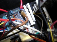
Had quite a setback last night upon power-up of my "amp #1" While diagnosing a no turn-on condition I had found resistor R506 open on the AC input board and replaced it with a Vishay Dale #CP00204R700JE14 along with the electrolytic capacitors on that board. I had previously done the audio input board wash and recap routine but removed the board again and checked every resistor and ended up replacing a few including all the fusible resistors as one or two were open if I remember correctly. Feeling quite good about my diligent efforts, I powered-up the amp and after a few seconds my replacement R506 popped in spectacular fashion! (see pictures) Quite an attention getter!! Obviously there is an issue yet undiscovered since the original R506 failed and now this one. Thoughts or ideas? 
Attachments

- Home
- Amplifiers
- Solid State
- Yet Another Adcom GFA-565 Thread