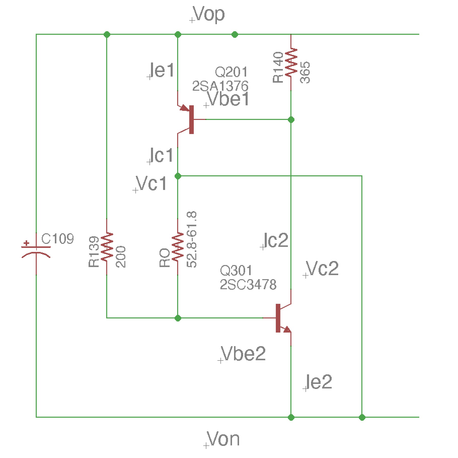
The above diagram has an error. The forum would not let me edit it for some reason. Here is the corrected diagram. I had not tied the collector of Q201 to the Von line.
Last edited:
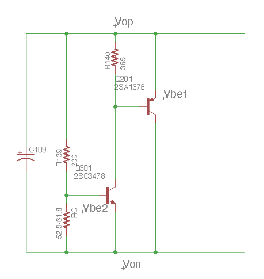
OK, so I tried to do this analytically, and it's fairly complicated. However, redrawing the circuit makes the basic conceptual operation easier to understand. Here's the same circuit after a bit of re-arranging. As you can see this is a pretty standard bias circuit for Q301, where the base voltage is set by the R139 and Ro divider. We know that Vbe is one of the more temperature dependent elements of a transistor, and most silicon transistors have a temperature coefficient of about -2 mV per degree C.
From this circuit, you can see that as the temperature of the junction of Q301 goes up, Vbe2 will go down, thereby increasing the current drawn through R139. The current through Ro will actually decrease, because the voltage across Ro (Vbe2) is lower, which means the base current of Q301 will increase. This will cause the collector current of Q301 yo increase, thereby increasing the current through Q201. This increased current will cause Vce of Q201 do decrease, which means Von and Vop will be pulled toward ground. This lower offset will then reduce the current through the output Darlingtons, thereby lowering the temperature.
What I am not clear about yet is how Q201 affects the circuit over temperature. As I recall one is mounted on the positive bank heatsink, and the other on the negative bank heatsink. The circuit does not appear to be symmetric relative to one heatsink versus the other, so, it is not clear that a decline in Vbe of Q201 will affect the circuit in the same way.
I suppose the mechanism may be that if Vbe1 goes down as the heatsink temp goes up, then the voltage on the collector of Q301 will go up, this will reduce the current through R140, but since the current through Q301 is set by the voltage divider R139 and Ro, this will cause the base current in Q201 to increase, thereby causing the bias offset on the output blocks to go down.
At a given temperature, increasing Ro will increase the base current in Q301, thereby reducing the bias offset on the output blocks, and reducing Ro will reduce the base current in Q301 thereby increasing the bias offset.
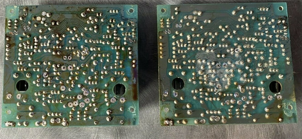
This is a laugh! Those are some of the worst boards I've seen. (Not my eBay post!)

Last edited:
Ha. I too saw those!
I guess the seller will be listing the original puked out capacitors for sale next 😀
Stay safe
Mayank
I guess the seller will be listing the original puked out capacitors for sale next 😀
Stay safe
Mayank
Yeah, I'm sure his listing will say something like "pre-puked" capacitors provide a much more "transparent" sound, since there is not all that messy electrolyte to get in the way!! And, as bonus, they can't leak again!
I got two better than those!! Not sure why I haven't thrown them away after replacing them with new boards. Maybe I should sell them on ebay 🙂
gabo
Disclaimer - I would never ever do something like that!!
gabo
Disclaimer - I would never ever do something like that!!
This is a laugh! Those are some of the worst boards I've seen. (Not my eBay post!)
LOL! I have a milk-crate full of crusty boards like this! I keep them around in case the parts start to become unobtainium. At least some of the transistors don't have electrolyte spittle on them.
Cogeniac, you might be interested to know, the GFA-585 has one NPN bias comp transistor mounted on the PNP side of the heatsink, and the PNP bias comp transistor sits on the input board! There is no bias comp transistor on the NPN side. I thought that was odd, but it works out somehow. The 585's bias is quite steady. One one of the GFA-585's I did, I actually ran another cable out to the heatsink, so it would be like the GFA-565 in that respect. It wasn't really any better as far as bias stability.
I don't know what this means to your investigation into the bias compensation, but it seems like it might be a clue.
Last edited:
I'm working on a couple amps and have a question on the LEDs in the constant current sources. At 3mA, I'm only seeing about 1.8v-1.9v, instead of 2.1v to 2.2v. When I look at various green LED specs, I don't see any with a Vf of 2.2v at 3mA If. Usually they need 8-10mA to get a Vf of 2.2v. Does anyone have an LED model that achieves that Vf at the If of this circuit? Thanks!
I'm having trouble finding LEDs with 2.1 Vf at a low (3mA) current so I'm going to adjust R146 (1.21K ohm) and R149 (825 ohm) to get 10mA drive through the LEDs, which will get the requisite 2.1V. That will also lower the rail voltages for the constant current source circuit, due to additional voltage drop across R153 and R154, but that shouldn't affect overall operation.
Lite-on part # LTL-1234A is what I use, and it gives very close voltage drops compared to the originals. It's listed in my parts list along with everything else.
D113 runs at about 0.7mA and D114 runs at 1.8mA.
D113 runs at about 0.7mA and D114 runs at 1.8mA.
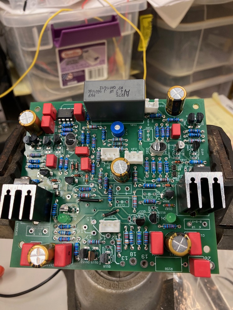
Okay, time to try version 4 of my Adcom board. The last one (sheesh 3 years ago!) worked fine, but had some mechanical fit issues. This one fixes those, although, building it up I identified a few very minor tweaks that I'll make in the next iteration. Hope to hook this board up to one of my amps over the next week or so. I'll report back. Got some very nice
<1mV matches for the input Darlingtons using the beta matcher board.
Considering adding a fail safe circuit to shut off the amp if the DC offset goes beyond the ability off the DC servo to correct it. Easy way to save $$$K speakers.
The two jumpers are to replace the Vishay trimmers I designed into the back side off the board. Not sure I'll need those, and they are very pricey ($16 each!!), but the real estate is there if I need them.
In this version, I copied Chris Hoppe copying my ECBE transistor footprint so the board can accommodate original or replacement parts with different pinouts. Nice to have that flexibility, even if it does make the board more crowded!
Last edited:
I'm so glad you fellas are continuing to work on these amplifiers for solutions. Please keep up the good work.
The ECBE arrangement was mine. 🙂 That was in the original beta matcher. I did give those boards out to various people who really needed them, I did not sell them. Thank you so much for sending me some, and each went to a good home.
-Chris
The ECBE arrangement was mine. 🙂 That was in the original beta matcher. I did give those boards out to various people who really needed them, I did not sell them. Thank you so much for sending me some, and each went to a good home.
-Chris
I'm so glad you fellas are continuing to work on these amplifiers for solutions. Please keep up the good work.
The ECBE arrangement was mine. 🙂 That was in the original beta matcher. I did give those boards out to various people who really needed them, I did not sell them. Thank you so much for sending me some, and each went to a good home.
-Chris
Ahh yes!! Sorry about that! Brilliant idea. I used it for all of the parts that have EBCE equivalents.
For this recent build, I got my Darlingtons to match at the sub 1 mV level. Fingers crossed.
Busy next week, so I'll try it out after that. Using a variac now.
S
@Cogeniac, Anatech and Phloodpants:
As an Adcom enthusiast, I have been following the thread assiduously for some time. From the early troubleshooting posts, I take it that it is probably best to remove the DC error amplifier IC, and then 'tweak/trim' the LTP so that DC balance is reached, and then restore the error amplifier IC so that a 'nudge' in the right direction will maintain DC balance and keep speaker-killing DC offsets at bay.
I am asking as I have a couple of GFA-545-II models that, over the years, showed erratic and high DC offsets. Replacing the LTP devices cured the issue, but I find that it is possible for the DC error amplifier to "lose grip" due to various factors.
I am banking on your vast experience and expertise to get some sane advice. Is it advisable to replace R616 with a 1k preset and trim the DC balance with the error amplifier IC removed? If not, what should be my approach to trim the DC offset to within the correction range of the error amplifier IC? Kindly help.
It would be great if Sir Scott could find the time to do a detailed "summing up" of his redesign of the bipolar current source (Post # 164), and its integration in the Adcom circuit, for the understanding of many of us who lack the engineering background to follow such stuff easily.
This has been one of the best "educational" threads that I have read in my life (I am a contemporary of Cogeniac!).
My humble salutes to the 'Gurus' !!
Attachments

I am not familiar with the GFA 545, but it looks a lot like the GFA-555.
I would NOT replace R616 with a pot, because that's going to throw the gain of the circuit off.
From the circuit posted, it doesn't look like the 545 is DC coupled, since the input stage, at least is running more or less single-ended class A. Can you post the entire schematic? The entire drive signal is created by Q614, which is then sent to the positive side power stage through R648, and gets inverted by Q618, and then the anti-phase signal goes out to the negative side power stage through R650. This means there is no ability to fix the DC offset until after Q614. I would assume that's what the VR602 pot is for. That op amp is not being used to compensate for DC offset. It looks like it is really just being used for audio feedback.
I DO like the idea of disabling the 565 Servo op amp when tuning the circuit, however.
In the 565, the servo basically samples the DC offset at the output, and creates an offsetting DC input at the input diff pairs. The DC offset is affected by many things between the input and the output, but one way to control it is to adjust the current sources for the TWO diff pairs. In my current version of the 565 board, I have provision for two multi-turn Vishay pots on the bottom side of the board. These are used to adjust the effective resistance of R144 and R145, in the current source circuit. Essentially, you can adjust out any imbalance in current between the positive and negative diff pairs. Doing that without the servo would make sense, since you want the un-servoed amplifier to be basically neutral, so adjusting out any imbalance and the activating the servo would make sense. I would do that by simply shorting the two inputs to the op-amp to generate zero output signal.
As I understand it, Phloodpants also matches the betas of the PNP and NPN diff pairs (a daunting task) to achieve the same basic result.
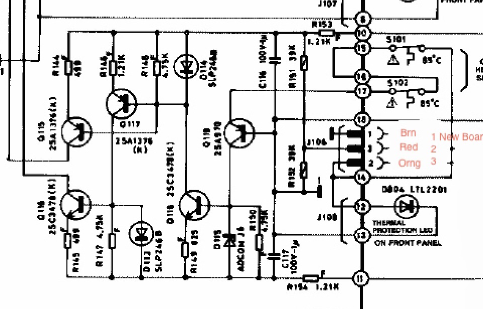
Here are the two circuit segments from the 565 schematic.
This is the input section. You can see there are Two opposite polarity diff pairs (!101/Q105 and Q102/Q106) each with a separate tail current line.
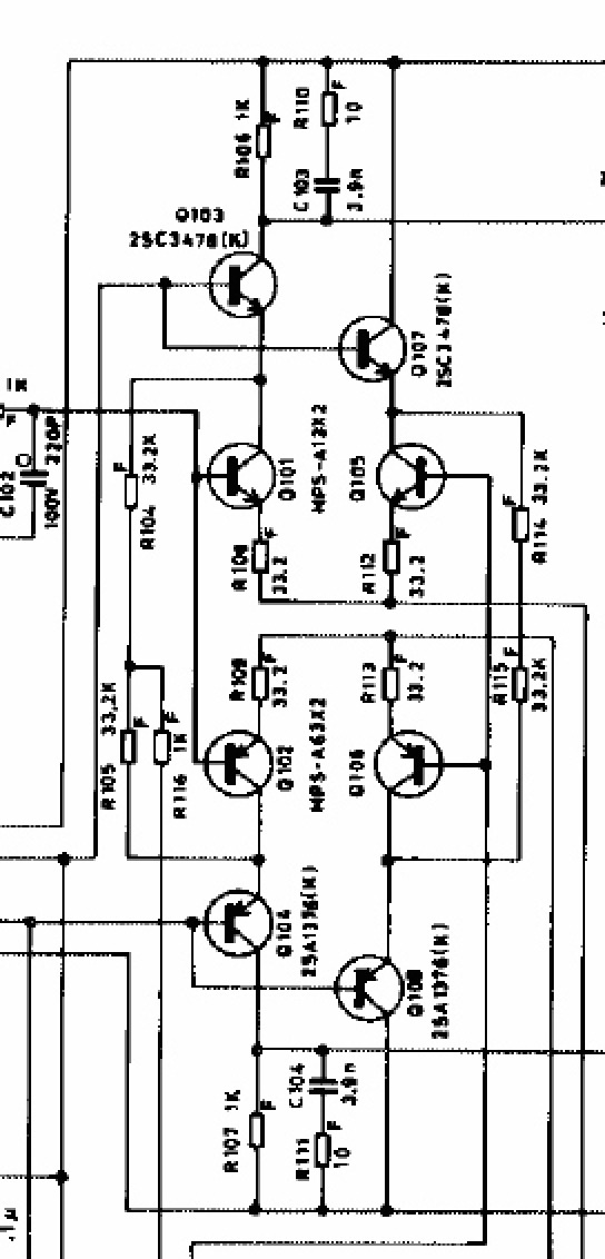
Those tail currents are set by the resistors R144 and R145 in the current source section below.
The other thought I have had relative to securing the output of the amp from high DC offsets, is to use the output of the servo to trigger a power shutdown circuit, so if the op amp gets to the point where it is close to railing, then the power supply just shuts off. Good way to save an expensive speaker system.
I would NOT replace R616 with a pot, because that's going to throw the gain of the circuit off.
From the circuit posted, it doesn't look like the 545 is DC coupled, since the input stage, at least is running more or less single-ended class A. Can you post the entire schematic? The entire drive signal is created by Q614, which is then sent to the positive side power stage through R648, and gets inverted by Q618, and then the anti-phase signal goes out to the negative side power stage through R650. This means there is no ability to fix the DC offset until after Q614. I would assume that's what the VR602 pot is for. That op amp is not being used to compensate for DC offset. It looks like it is really just being used for audio feedback.
I DO like the idea of disabling the 565 Servo op amp when tuning the circuit, however.
In the 565, the servo basically samples the DC offset at the output, and creates an offsetting DC input at the input diff pairs. The DC offset is affected by many things between the input and the output, but one way to control it is to adjust the current sources for the TWO diff pairs. In my current version of the 565 board, I have provision for two multi-turn Vishay pots on the bottom side of the board. These are used to adjust the effective resistance of R144 and R145, in the current source circuit. Essentially, you can adjust out any imbalance in current between the positive and negative diff pairs. Doing that without the servo would make sense, since you want the un-servoed amplifier to be basically neutral, so adjusting out any imbalance and the activating the servo would make sense. I would do that by simply shorting the two inputs to the op-amp to generate zero output signal.
As I understand it, Phloodpants also matches the betas of the PNP and NPN diff pairs (a daunting task) to achieve the same basic result.
Here are the two circuit segments from the 565 schematic.
This is the input section. You can see there are Two opposite polarity diff pairs (!101/Q105 and Q102/Q106) each with a separate tail current line.
Those tail currents are set by the resistors R144 and R145 in the current source section below.
The other thought I have had relative to securing the output of the amp from high DC offsets, is to use the output of the servo to trigger a power shutdown circuit, so if the op amp gets to the point where it is close to railing, then the power supply just shuts off. Good way to save an expensive speaker system.
Last edited:
@ Cogeniac:
That was fast! And thank you.
I thought I mentioned I needed some advice regarding the GFA-545-II, and that was the circuit I had attached. Matching devices to high tolerance is not easy for me for various reasons, including getting a large number of replacements. Here I am primarily interested in trimming the LTP circuit balance without affecting the gain, and then restore the dc servo.
Kindly go over the circuit and suggest a way out please. That would be an insurance for me, which would take care of things in the long run, I hope.
Thank you in advance, Sir.
Lucky timing. Sitting here in CA with a glass of wine, catching up on audio forums...
I think our posts and my edits crossed paths.
I never did implement the Post 164 current source. Got busy with other things and have only recently dug out my Adcom stuff, built a new board to the original circuit design, and started getting ready for a winter of restoring GFA 565's.
The Post 164 concept was aiming at assuring that the tail currents in the two diff pairs were always equal. That actually may not be that desirable. If the betas of the two pairs are not equal, then having the tail currents equal doesn't help. I think the original design, but with adjustability of the tail currents to fine tune the balance is probably best. That's how I have currently laid out the board.
@ Cogeniac:
That was fast! And thank you.
I thought I mentioned I needed some advice regarding the GFA-545-II, and that was the circuit I had attached. Matching devices to high tolerance is not easy for me for various reasons, including getting a large number of replacements. Here I am primarily interested in trimming the LTP circuit balance without affecting the gain, and then restore the dc servo.
Kindly go over the circuit and suggest a way out please. That would be an insurance for me, which would take care of things in the long run, I hope.
Thank you in advance, Sir.
As noted above, any offsets in the circuit are not a result of diff pair matching. The are a result of the bias circuits over on the right side. I would expect that, since that is all way after any real high voltage gain circuits, your high offset issues may be more to do with some other issues relative to Q614 and Q618.
Great! Enjoy that glass of vine!!
Yes, I get that regarding your mods. The important thing is the ability to tweak the 'raw' DC balance first, and then activate the servo.
Kindly suggest a way so that I could do the same with the simpler circuit of the GFA-545-II. ( I did not want to post the full circuit and appear to hijack the thread.) I would definitely like to have a way to null out the imbalances first--with your expert help!
Warm regards.
- Home
- Amplifiers
- Solid State
- Yet Another Adcom GFA-565 Thread