Re: Distortion vs. frequency
So THD20=1.65ppm? Based on your schematics, this is absolutely impossible.
Either your measurements or your schematics are wrong. In case of the latter, please no more pathetic reactions like this one:
Instead, show us the correct schematic.
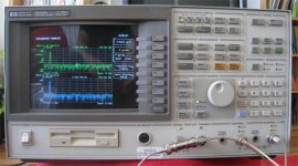
syn08 said:Finally, the YAP measured THD+N vs. frequency:
[snip]
So THD20=1.65ppm?
Based on your schematics, this is absolutely impossible.Either your measurements or your schematics are wrong. In case of the latter, please no more pathetic reactions like this one:
syn08 said:1. Take a deep breath.
2. Put your glasses on (if applies).
3. Open this: http://www.diyaudio.com/forums/show...058#post1596058
4. Look careful at the picture and try to identify the gate resistors. Hint: they are close to the 2SK1530/2SJ162 gate pins. If you don't know which is the gate pin just ask.
5. Identify the gate resistor values. A magnifier can come handy.
Instead, show us the correct schematic.
Re: Correction
Hi syn08,
I'm curious as to why you chose to generate the 19+20 kHz CCIF signal in this way, instead of the usual way of having two separate oscillators feeding an ultra-low distortion mixer.
Also, I'm not sure, but I suspect the details of the test signal you are making differ from those of the two individual tones in such a way that might matter. For example, the sidebands at 19 kHz and 20 kHz are somewhat synchronous as a result of the AM process. Also, I understand you to mean that you created the signals with a conventional amplitude-modulated process, as opposed to a double-sideband modulator, right?
Thanks,
Bob
syn08 said:
This paragraph should read:
Rather than mixing two 19KHz and 20KHz signals, the system 100% AM modulates a 19.5KHz carrier with a high purity 500Hz signal.
I should proofread before pressing submit...
Hi syn08,
I'm curious as to why you chose to generate the 19+20 kHz CCIF signal in this way, instead of the usual way of having two separate oscillators feeding an ultra-low distortion mixer.
Also, I'm not sure, but I suspect the details of the test signal you are making differ from those of the two individual tones in such a way that might matter. For example, the sidebands at 19 kHz and 20 kHz are somewhat synchronous as a result of the AM process. Also, I understand you to mean that you created the signals with a conventional amplitude-modulated process, as opposed to a double-sideband modulator, right?
Thanks,
Bob
Re: Re: Re: Re: Damping Factor
Hehe 😉
janneman said:
Lucky you! This is one great piece of equipment. Looking forward to your findings.
Hehe 😉
Attachments
Re: Re: Correction
Bob,
I did not create a thing; this is how the 19+20KHz test signal is generated by the Amber 5500 IMD extension/option board. This option allows reading the IMD values straight on the instrument's digital display (and through the GPIB interface).
Honestly, I haven't looked closely on how this AM and carrier supression is accomplished in the option board. I have the schematics and I'll take a closer look ASAP (I could also post the schematic for the perusal of the telecom savvy engineers around). What I know for sure is that I am feeding the spectrum analyzer with the Amber 500 "Measured Function" signal, which specially designed for spectral analysis.
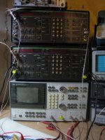
I have compared the Amber 5500 IMD measurement results with the classic approach you mentioned (I have actually two Amber instruments - see attached picture - and I used them to generate high purity 19KHz and 20KHz signals, mixing them either straight into 50ohm or in a AD797 opamp) and I got in either case no statistically different IMD results. Actually I prefer the 50ohm mixing, because extracting the AD797 noise and distortion contribution is a very time consuming process which, unfortunately, I was unable to find a way to automatize. I would need a very low noise programmable switching matrix, which is expensive (at least from Agilent or Keithley that I know about).
Bob Cordell said:
Hi syn08,
I'm curious as to why you chose to generate the 19+20 kHz CCIF signal in this way, instead of the usual way of having two separate oscillators feeding an ultra-low distortion mixer.
Also, I'm not sure, but I suspect the details of the test signal you are making differ from those of the two individual tones in such a way that might matter. For example, the sidebands at 19 kHz and 20 kHz are somewhat synchronous as a result of the AM process. Also, I understand you to mean that you created the signals with a conventional amplitude-modulated process, as opposed to a double-sideband modulator, right?
Thanks,
Bob
Bob,
I did not create a thing; this is how the 19+20KHz test signal is generated by the Amber 5500 IMD extension/option board. This option allows reading the IMD values straight on the instrument's digital display (and through the GPIB interface).
Honestly, I haven't looked closely on how this AM and carrier supression is accomplished in the option board. I have the schematics and I'll take a closer look ASAP (I could also post the schematic for the perusal of the telecom savvy engineers around). What I know for sure is that I am feeding the spectrum analyzer with the Amber 500 "Measured Function" signal, which specially designed for spectral analysis.
I have compared the Amber 5500 IMD measurement results with the classic approach you mentioned (I have actually two Amber instruments - see attached picture - and I used them to generate high purity 19KHz and 20KHz signals, mixing them either straight into 50ohm or in a AD797 opamp) and I got in either case no statistically different IMD results. Actually I prefer the 50ohm mixing, because extracting the AD797 noise and distortion contribution is a very time consuming process which, unfortunately, I was unable to find a way to automatize. I would need a very low noise programmable switching matrix, which is expensive (at least from Agilent or Keithley that I know about).
Attachments
myhrrhleine said:How does YAP sound?
especially compared to lowly 100PPM distorted amps?
This is TBD, after the construction will be completed. I my constructions, typically the signal path is around 30% of the total complexity, so there are many things to decide, starting with the PS (still pondering between a classic and separate SMPSs based on the TI UCC3895 phase shift PWM controller) and ending up with the enclosure. All these are going to happen over the next four to six months, then the audition test are going to happen. Meantime, you may want to read about the listening results for the PGP amp http://synaesthesia.ca/listening.html
Honestly, I do not expect any major listening differences to the PGP amp, while a comparison with less performant amps, as you mentioned, is not in the scope of my work.
syn08 said:.............
so there are many things to decide, starting with the PS (still pondering between a classic and separate SMPSs based on the TI UCC3895 phase shift PWM controller
...........................
Ah, you still remember my suggestion! 🙂 I assume that you also know that a few forum members have done some experiments with this chip.
BTW, an article about an audio SMPS (type: SAPS-400, not UCC3895 based) was published in Elektor, June 2008, but I have my doubt whether this PSU will meet with your standards (not mine, anyhow) See:
http://www.elektor.com/magazines/2008/june/saps-400.495049.lynkx
And also this!:
http://amplioaudio.blogspot.com/2008/02/web-anonymity-bites-back.html
http://www.diyaudio.com/forums/showthread.php?s=&threadid=116819&perpage=25&pagenumber=1
http://www.diyaudio.com/forums/showthread.php?postid=1354569#post1354569
I can not think of
using Switching Mode Power Supply (smps) for my audio circuits.
I am sure they can do good. Nowadays.
But just do not ever tell me go this way in my power amplifiers.
Because it is no use. I wont go there !!!! 😎
Call me Old fashion.
Call me Analog fundamentalist.
.. does not matter ..
Call me Anything
You still got to serve somebody.
It may be The Devil (digital) or it may be The Lord (analog audio)
... but you still got to serve some body.
It is bad enough they (the music industry) have forced me
to get music in CD format, compact digital discs.
With playing devices having Digital to Analog Conversions units inside.
In my mind they are heading all the wrong way with all this.
And some 'fools' jump on their train 😀
My god! Can't they understand ... what they are doing.
But Always look at the Bright Side of Life:
Just you wait some 30-40 years. (I might be dead and gone)
Then there will be some turning back to All Analog Systems again.
You just wait and see this Prophet from Sweden
being all right .. in some distant future.
History does not always go in one line from past to future.
Some times it goes in circle.
There are turning backs.
And we some times will be again where we were, once before.
Analog Audio Regards
Lineup, the audio philosopher
.
using Switching Mode Power Supply (smps) for my audio circuits.
I am sure they can do good. Nowadays.
But just do not ever tell me go this way in my power amplifiers.
Because it is no use. I wont go there !!!! 😎
Call me Old fashion.
Call me Analog fundamentalist.
.. does not matter ..
Call me Anything
You still got to serve somebody.
It may be The Devil (digital) or it may be The Lord (analog audio)
... but you still got to serve some body.
It is bad enough they (the music industry) have forced me
to get music in CD format, compact digital discs.
With playing devices having Digital to Analog Conversions units inside.
In my mind they are heading all the wrong way with all this.
And some 'fools' jump on their train 😀
My god! Can't they understand ... what they are doing.
But Always look at the Bright Side of Life:
Just you wait some 30-40 years. (I might be dead and gone)
Then there will be some turning back to All Analog Systems again.
Fashion of The Day comes and goes in cycles.
The 60-ies Andy Warhol came back.
Tubes has come back.
Analog Audio will come back.
You just wait and see this Prophet from Sweden
being all right .. in some distant future.
History does not always go in one line from past to future.
Some times it goes in circle.
There are turning backs.
And we some times will be again where we were, once before.
Analog Audio Regards
Lineup, the audio philosopher
.
Re: Re: Re: Re: Re: What could be done better...
Based on accurate BSIM3 and EKV models, a Vgd mismatch of 10mV at 150mA, results also practically in an Id difference of 10mA.
Whether you like it or not, such a mismatch is definitely NOT critical.
In my OPS with four pair of MOSFETs, even a mismatch of plus and minus 20mV has a negligible effect on the distortion, that is, at full power and at 2W. So your fear for adverse effects is based on nothing more than a wild guess.
syn08 said:.................
2. That is correct at 5A, I was thinking about low current. 50mA at 5A makes theoretically about 10mA at 150mA (practically the dispersion is about double because of the subthreshold current dispersion contribution and a few other things), that is say 14% and this is assuming the errors are cumulating on the same side (is it +/-5mV or +/-10mV?). It may or may not be critical, but I certainly don't like it. Isn't it the few first watts that define the amp quality? When the drain current is 5A and the SPL out of my speakers reaches 110dB, I think I can forget about any 50mA mismatches anyway.
..................
Based on accurate BSIM3 and EKV models, a Vgd mismatch of 10mV at 150mA, results also practically in an Id difference of 10mA.
Whether you like it or not, such a mismatch is definitely NOT critical.
In my OPS with four pair of MOSFETs, even a mismatch of plus and minus 20mV has a negligible effect on the distortion, that is, at full power and at 2W. So your fear for adverse effects is based on nothing more than a wild guess.
Edmond Stuart said:
Sure, its pretty fast, almost as fast as Stochino's amp (300V/us). But don't think it's due to that exotic diamond buffer, rather C34, that remedies the inherent shortcomings of a diamond buffer. Without that cap the performance falls below mediocrity: rising SR=28V/us, falling SR=13V/us (approximately).
Cool, that's what I get from a quick calc ( Vc=(Ic/c)t ), hence my previous comments in this thread WRT C34 being required to prevent the B-E junctions of the driver transistors being reverse biased when you are left with the current source to charge the MOSFET input capacitance.
BTW, do your MOSFET models accurately simulate the rise in Cin due to Cgd at high Id?
Cheers,
Glen
G.Kleinschmidt said:BTW, do your MOSFET models accurately simulate the rise in Cin due to Cgd at high Id?
For the ones I created, Cgs is modeled as being constant with Vgs, while Cgd vs. Vgd is a "best fit" in the least squares sense to the datasheet curves of Crss (=Cgd) vs Vgd. The Cds (=Coss-Crss) variation is modeled with the varying capacitance of the body diode.
The end result of the Cgd variation is that the simulated small-signal bandwidth is a lot less near clipping than it is with 0 Volts DC out because of increasing Cgd as Vgd gets small. For the Cgd variation, a nonlinear capacitance model was used as a subcircuit element. The function used for fitting is described in the LTspice documentation for the LTspice-specific VDMOS model used for vertical MOSFETs. See the Cgd graph in that documentation for details.
Re: Re: Re: Re: Re: Re: What could be done better...
I’m still having difficulties getting these models working in LTspice and the models I have don’t seem to simulate Cin at high Id properly.
WRT to my previous post (if it, or this one, for that matter, appears 🙄) - there is an utterly ridiculous delay between me posting and a thread appearing due to being "under moderation". (Calling puerile rubbish puerile rubbish is apparently classified as “abuse” around here, even when it is directed at you ).
).
I can’t edit posts either – LOL!
I’m not going to put up with this stupidity (I guess that’s the whole idea). Send me an email instead.
Cheers,
Glen
Edmond Stuart said:
Based on accurate BSIM3 and EKV models, a Vgd mismatch of 10mV at 150mA, results also practically in an Id difference of 10mA.
Whether you like it or not, such a mismatch is definitely NOT critical.
In my OPS with four pair of MOSFETs, even a mismatch of plus and minus 20mV has a negligible effect on the distortion, that is, at full power and at 2W. So your fear for adverse effects is based on nothing more than a wild guess.
I’m still having difficulties getting these models working in LTspice and the models I have don’t seem to simulate Cin at high Id properly.
WRT to my previous post (if it, or this one, for that matter, appears 🙄) - there is an utterly ridiculous delay between me posting and a thread appearing due to being "under moderation". (Calling puerile rubbish puerile rubbish is apparently classified as “abuse” around here, even when it is directed at you
). I can’t edit posts either – LOL!
I’m not going to put up with this stupidity (I guess that’s the whole idea). Send me an email instead.
Cheers,
Glen
Glen, the 2SJ201/2SK1530 EKV models I created are messed up in LTspice. It's probably better to use Edmond's BSIM models. I've attached the LTspice versions of these below.
That said, it's not Id that's the critical parameter for input capacitance variation, but Vgd.
That said, it's not Id that's the critical parameter for input capacitance variation, but Vgd.
Attachments
Re: Re: Re: Re: Re: Re: Re: What could be done better...
Glen,
As far as I recall, Andy has these models up and running for LTSpice.
Regarding the MOSFET matching, I'm not sure what the issue appears to be (E. is on my ignore list) but certainly something sounds fishy with the models (or models usage). What I was trying to explain is that if you are matching devices for Vgs = Vt+/-10mV @Id =150mA, then at Id = 5A the Id variation for +/- 10mV is much larger. I can proof this mathematically, but there's little reason to bother. Enough to recall that Id=f(Vgs) is parabolic. That is, the same variation of Vgs at low current has a much larger impact at large current.
It can be easily shown that a Vgs variation of "e" volts creates a drain current variation of Ie=2*K*(Vgs-Vt)*e Now plug in some numbers from the data sheet (Vgs=2.8V at Id=5A and Vt=0.8V and a transconductance of 5S and you'll get Ie=400mA. If you consider +/-10mV you'll get a spread of (worst case) 800mA. Is this a lot, that is, having an about +/-10% current imbalance in the output devices acceptable? This I don't know for sure, but intuitively I believe it is not.
Regarding the other question regarding C34. Even mr. Ignored acknowledged that it's the diamond buffer that helps discharging the charge (through the CC sources). Of course C34 helps as well! However, the same ignored omniscient claims that C34 helps turning on which I am still having some troubles understanding as of why. Just to figure it out, I removed C34 from one of the boards and the rise and fall times remained equal and increased from 150nS to about 250nS, rendering a slew rate of 160V/uS (comparing to 270 V/uS).
Edit: I've noted that Andy just posted the LTSpice models.
G.Kleinschmidt said:
I’m still having difficulties getting these models working in LTspice and the models I have don’t seem to simulate Cin at high Id properly.
WRT to my previous post (if it, or this one, for that matter, appears 🙄) - there is an utterly ridiculous delay between me posting and a thread appearing due to being "under moderation". (Calling puerile rubbish puerile rubbish is apparently classified as “abuse” around here, even when it is directed at you
I can’t edit posts either – LOL!
I’m not going to put up with this stupidity (I guess that’s the whole idea). Send me an email instead.
Cheers,
Glen
Glen,
As far as I recall, Andy has these models up and running for LTSpice.
Regarding the MOSFET matching, I'm not sure what the issue appears to be (E. is on my ignore list) but certainly something sounds fishy with the models (or models usage). What I was trying to explain is that if you are matching devices for Vgs = Vt+/-10mV @Id =150mA, then at Id = 5A the Id variation for +/- 10mV is much larger. I can proof this mathematically, but there's little reason to bother. Enough to recall that Id=f(Vgs) is parabolic. That is, the same variation of Vgs at low current has a much larger impact at large current.
It can be easily shown that a Vgs variation of "e" volts creates a drain current variation of Ie=2*K*(Vgs-Vt)*e Now plug in some numbers from the data sheet (Vgs=2.8V at Id=5A and Vt=0.8V and a transconductance of 5S and you'll get Ie=400mA. If you consider +/-10mV you'll get a spread of (worst case) 800mA. Is this a lot, that is, having an about +/-10% current imbalance in the output devices acceptable? This I don't know for sure, but intuitively I believe it is not.
Regarding the other question regarding C34. Even mr. Ignored acknowledged that it's the diamond buffer that helps discharging the charge (through the CC sources). Of course C34 helps as well! However, the same ignored omniscient claims that C34 helps turning on which I am still having some troubles understanding as of why. Just to figure it out, I removed C34 from one of the boards and the rise and fall times remained equal and increased from 150nS to about 250nS, rendering a slew rate of 160V/uS (comparing to 270 V/uS).
Edit: I've noted that Andy just posted the LTSpice models.
- Status
- Not open for further replies.
- Home
- Amplifiers
- Solid State
- YAP - Yet Another PowerAmp