Happy New Year!
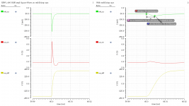
One more plot from the square wave with and without stabilising caps. The supply current, out of an ideal source, VDD_S : P, the output common mode OUT_CM and the output diff more OUT_DIFF. The plot on the left is without the slow-down stabilising caps. The current pulse is very very quick and likely to set up a longer lasting ripple effect on the supply. Not that this amplifier should be very sensitive to supply ripple, but it doesn't look pretty. The output common mode may be rejected by the earphone, but again it is not looking pretty.
Best Regards
Jens
Attachments
The Stax commercial amps all have 100kHz bandwidth (-3dB).
If you drive a square wave through one of those, you expect to see high current spikes.
(The Stax headphones are like 150p capacitors.)
The pulse current likely comes from the power supply caps than e.g. a regulator.
So I do not understand what the problem is ?
Happy New Year,
Patrick
If you drive a square wave through one of those, you expect to see high current spikes.
(The Stax headphones are like 150p capacitors.)
The pulse current likely comes from the power supply caps than e.g. a regulator.
So I do not understand what the problem is ?
Happy New Year,
Patrick
Hi Patrick,
Yes, power supply caps will supply the current spikes. I just like things to be a bit less highly strung, that's all. My concern is the relatively poor predictability of actual circuit performance given that the models are so-so (the NMOS output device is using the model for a different part number, for instance, with hacks for DC operation, but nothing for capacitances). If I insert explicit capacitances which keeps internal signals out of saturation, I feel less worried. That's all.
I actually very carefully ran a slightly complicated linearity simulation with and without those caps and got only double the distortion (from very low to quite low), so I cannot claim to have a strong indication that the amp is working badly without those caps. But I enjoy checking things as carefully as I know how.
Best Regards
Jens
So, complicated linearity simulation.
Back in the 1970s, a measure other than THD was introduced to describe how well amplifiers did for HiFi. The idea was that if internal stages ran into slew rate limitation linearity would not be ensured. The problem would not show up when an amplifier was only stimulated by one or more sine waves signals.
The paper "A Method for Measuring Transient Intermodulation Distortion" by Leinonen, Matti and Curl describes it better than I could.
The input signal: A sum of a low frequency square wave and a higher frequency sine wave (at a lower amplitude) creates intermodulation products inside the audio band and the magnitude of those intermodulation products increase sharply if the amplifier is not running inside properly biased regions for crucial devices. In the article, two frequency ratios are proposed, sqrt(4 * sqrt(20)) and sqrt(5 * sqrt(20)). The latter is used in the article, with the frequencies being 3.18 kHz and 15 kHz.
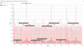
I use the lower ratio, giving me 3.66 kHz and 15.48 kHz. In order to get a nice clean Fourier analysis, I use an analysis time internal which gives me the fundamental of all the signals. The input signals, and the intermodulation products, are then harmonics of that fundamental and I can get frequency plots with no smearing. Or low enough smearing, anyway. I picked 60 Hz as the fundamental and the 61st and 258th harmonics as input frequencies (258/61 is pretty close to sqrt(4 * sqrt(20)) ). In this way, I arrive at a 3.66 kHz square wave and a 15.48 kHz sine wave. By using 16.6666666 ms span of signal in the Fourier analysis and no window (aka "rectangular window"), I get nicely defined results of the frequency analysis. There are many more spikes in the Fourier analysis results than the input fundamental (for the sine wave) and the harmonics of the square wave, but the spot frequencies I need are giving low enough levels that the analysis gives me confidence. The number of points in the Fourier analysis is 2^17, giving 7.9 MHz as the analysis sampling frequrency. Since I did not low-pass filter any of the signals going into the Fourier analysis, there are a lot of spurious tones. Looking at the DIM_Inp_Frq plot we see markers on the frequencies which are inside the audio band. I calculate the frequencies using Octave
If you look at the markers, you will see some intermod products at a low level (0.3 uV) and others at very low levels (less than 10 pV) for an input amplitude of 0.125 V. The analysis of the linearity is then the square root of the power of all the intermodulation signals divided by the amplitude of the low frequency fundamental
So, the input signal (which should be ideal) has 0.0004 % DIM distortion. Oh well.
Back in the 1970s, a measure other than THD was introduced to describe how well amplifiers did for HiFi. The idea was that if internal stages ran into slew rate limitation linearity would not be ensured. The problem would not show up when an amplifier was only stimulated by one or more sine waves signals.
The paper "A Method for Measuring Transient Intermodulation Distortion" by Leinonen, Matti and Curl describes it better than I could.
The input signal: A sum of a low frequency square wave and a higher frequency sine wave (at a lower amplitude) creates intermodulation products inside the audio band and the magnitude of those intermodulation products increase sharply if the amplifier is not running inside properly biased regions for crucial devices. In the article, two frequency ratios are proposed, sqrt(4 * sqrt(20)) and sqrt(5 * sqrt(20)). The latter is used in the article, with the frequencies being 3.18 kHz and 15 kHz.
I use the lower ratio, giving me 3.66 kHz and 15.48 kHz. In order to get a nice clean Fourier analysis, I use an analysis time internal which gives me the fundamental of all the signals. The input signals, and the intermodulation products, are then harmonics of that fundamental and I can get frequency plots with no smearing. Or low enough smearing, anyway. I picked 60 Hz as the fundamental and the 61st and 258th harmonics as input frequencies (258/61 is pretty close to sqrt(4 * sqrt(20)) ). In this way, I arrive at a 3.66 kHz square wave and a 15.48 kHz sine wave. By using 16.6666666 ms span of signal in the Fourier analysis and no window (aka "rectangular window"), I get nicely defined results of the frequency analysis. There are many more spikes in the Fourier analysis results than the input fundamental (for the sine wave) and the harmonics of the square wave, but the spot frequencies I need are giving low enough levels that the analysis gives me confidence. The number of points in the Fourier analysis is 2^17, giving 7.9 MHz as the analysis sampling frequrency. Since I did not low-pass filter any of the signals going into the Fourier analysis, there are a lot of spurious tones. Looking at the DIM_Inp_Frq plot we see markers on the frequencies which are inside the audio band. I calculate the frequencies using Octave
octave:1> f0=60
f0 = 60
octave:2> f1=61*f0
f1 = 3660
octave:3> f2=258*f0
f2 = 15480
octave:4> dim_fs = abs([f2 - f1*(1:9)])
dim_fs =
   11820    8160    4500     840    2820    6480   10140   13800   17460
If you look at the markers, you will see some intermod products at a low level (0.3 uV) and others at very low levels (less than 10 pV) for an input amplitude of 0.125 V. The analysis of the linearity is then the square root of the power of all the intermodulation signals divided by the amplitude of the low frequency fundamental
octave:8> dim_mags_in = [314e-9, 5.8e-12, 313e-9, 6.6e-12, 313e-9, 5.9e-12, 312e-9, 8.2e-12, 313e-9]
octave:17> v2 = 0.127
octave:18> 100*sqrt(sum(dim_mags_in .^ 2))/v2
ans = 5.5110e-04
So, the input signal (which should be ideal) has 0.0004 % DIM distortion. Oh well.
Attachments
Transient Intermodulation Distortion simulation, continued
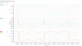
The output signal. The 400_DIM_Out_Tim plot shows the waveforms, OUT_DIFF at the top, swinging 800 Vdiff pp, OUT_CM in the middle swinging less than 1 Vdiff pp and the two polarities OUTN and OUTP. The signal is, as described, a low frequency square wave (loud signal) and a high frequency sine wave (weak signal).
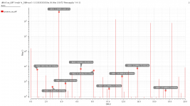
The frequency components are picked from the Fourier result shown in 400_DIM_Out_Frq plot. Using the Big Calculator (Octave) I get
So, for max output amplitude, we get 0.03% DIM. That's certainly a respectable result going by the article cited above. Harmonic distortion is higher, but is not frightening me (dominated by HD3)
I would like to note that in spite of all my talk of slew rate limitations and stabilising capacitors and so on, I do not get bad results for neither THD nor DIM when playing around with these dimension choices. I get double the DIM if I remove all stabilising and filtering capcitors, and smaller distortion of both types for more degenerated input transistor pairs (i.e. if I stay with the lower input device bias current as in the two designs at the beginning of this thread). The low number of stages, modest degree of feedback and massive bandwidth are all working in our favour.
So, this amplifier is a robust design giving good results in this test. I like it.
Best Regards
Jens
The output signal. The 400_DIM_Out_Tim plot shows the waveforms, OUT_DIFF at the top, swinging 800 Vdiff pp, OUT_CM in the middle swinging less than 1 Vdiff pp and the two polarities OUTN and OUTP. The signal is, as described, a low frequency square wave (loud signal) and a high frequency sine wave (weak signal).
The frequency components are picked from the Fourier result shown in 400_DIM_Out_Frq plot. Using the Big Calculator (Octave) I get
octave:21> v2 = 408.2
octave:5> dim_fs = abs([f2 - f1*(1:9)])
octave:20> dim_mags_out_d = [20.8e-3, 53.1e-3, 7.1e-3, 60.1e-3, 4.35e-3, 66.8e-3, 3.1e-3, 72.9e-3, 2.4e-3]
octave:22> 100*sqrt(sum(dim_mags_out_d .^ 2))/v2
ans = 0.031682
So, for max output amplitude, we get 0.03% DIM. That's certainly a respectable result going by the article cited above. Harmonic distortion is higher, but is not frightening me (dominated by HD3)
| Output Amplitude, Vdiff p-p | HD3 | DIM |
| 100 V | 0.01% | 0.002% |
| 400 V | 0.3% | 0.03% |
I would like to note that in spite of all my talk of slew rate limitations and stabilising capacitors and so on, I do not get bad results for neither THD nor DIM when playing around with these dimension choices. I get double the DIM if I remove all stabilising and filtering capcitors, and smaller distortion of both types for more degenerated input transistor pairs (i.e. if I stay with the lower input device bias current as in the two designs at the beginning of this thread). The low number of stages, modest degree of feedback and massive bandwidth are all working in our favour.
So, this amplifier is a robust design giving good results in this test. I like it.
Best Regards
Jens
Attachments
And components.
Resistor types. The feedback resistors look nice in a Bourns thick film type; low inductance, isolated screw mount to go directly onto heatsink. The output degeneration resistors do not need to be low inductance, maybe 2W Kiwame resistors?
I ran a noise analysis to find out which resistors contribute the most to the output noise. My "thinking" was that since power of noise is relatively the same for all resistors, the resistors which contribute the most to output noise are the ones where whatever errors they introduce are the most important. The winner, by a country mile, was the input degeneration resistors. I guess it makes sense, their value defines the gain of the input. Anyway, if you feel there is a need to have an origin story for some components, the input degen R5, R6, R7 and R8, are the ones to tell it about. According to my unsubstantiated gut feel.
Capacitors: the slow down caps are small enough that silver Mica caps are available in their sizes. That sounds nice. Film caps are going to work fine, I'm sure.
Power ratings. A lot of resistors are dissipating not a lot, but a few stick out. If we take the DC operating point in both full output and idle, we get the power dissipated in each. The power supply and output MOSFETs dissipate enough that they need heatsink mount, of course. The thermistor part of R9, R10, R19, R20 dissipate near enough nothing, but I'll mount them on the heatsink (some of the thermistors come in an isolated screw terminal form factor, and connecting wires, ready to be bolted onto the heatsink). The cascode devices will need a heatsink small enough to be mounted on the PCB (not the main heatsink) if that makes for a simpler PCB layout.
The input devices are not dissipating a lot, I picked 20V for the cascode voltage, but temperature stability is more likely when they are connected together in a thermal sense. The winning suggestion, IMHO, is Ring Terminals (Matt's tech pages) which I can then connect back to back with a bolt.
| Name | Power (DC) |
| R21, R22, R23, R34 | 4 W |
| R15, R16, R17, R18 | 0.5 W |
| Q1, Q2, Q3, Q4 | 2 W |
Oooh, Pretty. Using KiCAD 6, the automatic library symbol download thingie at Mouser (other vendors too, I'm sure) does simplify things.
Best Regards
Jens

Best Regards
Jens
Carrying on.
The 580V bias is inspired by various projects on other forums, "just" a constant current into a bunch of Zener diodes. The depletion NMOS FET is available, and I'm sure it will do well. Safety resistor in the output, and a resistor to discharge the filter cap when powered off (so I can poke my fat fingers into the box without getting my affairs in order first...).
I'm making it 450 V AC transformer secondary, 635 V peak after rectifier, 4 mA into load and 10 uF filter cap => 4 V ripple before Constant Current transistor. (OK, the cap is larger than it needs to be.) 100 kOhm R and 0.1 uF C twice in the filter circuit and 5 MOhms for safety's sake in the output.
For the regulated amplifier supplies, I'm staying with the circuit from Hesener, just using a Zener diode for the PNP base bias, and using the same MOSFETS as the amplifier for output.
Best Regards
Jens
I am sure you know those MOSFETs are now unobtanium,
either extremely long leadtime, or obsolete.
So maybe time to consider alternative devices.
Patrick
either extremely long leadtime, or obsolete.
So maybe time to consider alternative devices.
Patrick
Hi Patrick,
Yes, the ones used for ever and ever on the other boards are. However, a slightly different depletion mode NMOS is still in stock.
IXYS IXTP1R6N100D2
I will be ordering soon 😎
Best Regards
Jens
Yes, the ones used for ever and ever on the other boards are. However, a slightly different depletion mode NMOS is still in stock.
IXYS IXTP1R6N100D2
I will be ordering soon 😎
Best Regards
Jens
Here the bias supply I made, essentially a shunt regulator using the TL431. Please disregard the MOSFET part number, in fact I used a 1200V IGBT , mostly because I had some 😀
By changing the divider ratio (R2 + R3 --> 10k potentiometer), the bias voltage can be adjusted up and down. In my build, I set the range to 200V...600V. Have yet to play with this some more to get a better understanding of the impact.
Just as a proposal, you can use a regular enhancement mode in combination with a LM317, there should be a proposal in the 317 datasheet for that. You may lose in input resistance (isolation from line noise) but with that huge lowpass in the output towards the headphone it doesnt really matter....
Attachments
Hi Hesener,
Yes, I did have a look. I think I like the simpler Zener diode based solution. I'm not sure the constant current is particularly needed, but it will cut down on noise. As you say, the bias is filtered a lot.
For the amplifier supply, I'm ending up on your proposal. I did have to get a spreadsheet going to convince myself that I wasn't going to blow up anything when the mains voltage changes (+/- 10%? The Outrage!).
Actually, for the bias, the transformer probably needs a 480 V secondary to always produce enough level (in my schematic above), and the cap rating should be higher, above 750V.
Best Regards
Jens
and the positive regulated supply.
The 300 V Zener diode across the NPN is just in case. The 40 uF DC cap is sized so that I get 20 Vpp ripple with 80 mA current draw, which is 55 mA into the amp and 15 mA (typ) into the regulator and support, plus margin. With 20 V ripple, I get max volts at bridge output to be 360 V with mains 10% high and min voltage to be 270 V with -10% and ripple. The 3k9 series resistor then dissipates 1 W, the NPN 3 W and the regulator 0.13 W, for nominal mains voltage. Gate and base resistors because they are a good idea in the main amp..

Best Regards
Jens
PS Explaining stuff here really helps me double check. For instance, I had gone for a 1% different voltage divider at the regulator input, until I remembered the bias current going into the reference input which turns out to be close to... 1% of the current going into the lower part of the divider. So, the original value was better 🙂
The 300 V Zener diode across the NPN is just in case. The 40 uF DC cap is sized so that I get 20 Vpp ripple with 80 mA current draw, which is 55 mA into the amp and 15 mA (typ) into the regulator and support, plus margin. With 20 V ripple, I get max volts at bridge output to be 360 V with mains 10% high and min voltage to be 270 V with -10% and ripple. The 3k9 series resistor then dissipates 1 W, the NPN 3 W and the regulator 0.13 W, for nominal mains voltage. Gate and base resistors because they are a good idea in the main amp..
Best Regards
Jens
PS Explaining stuff here really helps me double check. For instance, I had gone for a 1% different voltage divider at the regulator input, until I remembered the bias current going into the reference input which turns out to be close to... 1% of the current going into the lower part of the divider. So, the original value was better 🙂
And finally getting all the component / footprint libraries put together in the PCB tool. Phew! The big order at Mouser has been paid for, so just need to draw up (and have made) the PCBs. Oh and transformer. And box.
Anyway, one thing at a time.
580V Pro bias: front, back and 3D view. All thanks to KiCAD. 150mm x 40mm. Not exactly compact, but better to space out components in this actually reasonably high voltage circuit. The footprints are sometimes a little generous (23 mm for a 1/8 W resistor?), they might need trimming for the amplifier. The wire connectors might be a bad choice (1x1mm pins, recommended if you don't know what your want).
Best Regards
Jens
Beautiful! Just one Remark, the connection between Z150-2 and Z150-3 seems quite close to other traces, and the voltages are elevated. Calll me paranoid buti do like large creepage and clearance, 3x...4x if i have the space and it doesnt add Cost....
Thanks. The tool makes it easy - no comparison to the tape-and-scalpel work of 30 years ago.
I also found a better way to do a diode bridge (also a place with plenty of voltage difference), so a little more space was available.
What I want to do when I get the PCBs back is to drill holes under the elements which dissipate a little. The Zener diodes in this schematic dissipate 600 mW. So, a 4mm hole in the PCB underneath should allow for a little more air to move, helped by mounting the diodes with a little standoff.
Best Regards
Jens
All boards done!
A single channel, to fit in 220 x 120mm (for a Mini Dissipante 3U 250 case). Power devices mounted on heatsink and legs bent up to meet PCBs. Room for some very nice double TO-92 heatsinks for the input devices 🙂. The feedback resistors also on heatsink - thin-film 25W devices - just completely won me over, not expensive, very low inductance and heatsink mount.
Star routing of GND connections.

Best Regards
Jens
A single channel, to fit in 220 x 120mm (for a Mini Dissipante 3U 250 case). Power devices mounted on heatsink and legs bent up to meet PCBs. Room for some very nice double TO-92 heatsinks for the input devices 🙂. The feedback resistors also on heatsink - thin-film 25W devices - just completely won me over, not expensive, very low inductance and heatsink mount.
Star routing of GND connections.
Best Regards
Jens

Just one more thing...
Hesener mentioned high voltage and component clearance. I did have track spacing on my list of things to worry about, and finally got 'round to beginning to inform myself.
Good thing, too. Really helpful links include a calculator: pcbtracespacing and a discussion on KiCAD forum: trace-separation which does mention that it's unknown how device manufacturers expect safe equipment to be built which comes close to 800V / 1000V voltage difference across pins of a device in a TO-220 package.
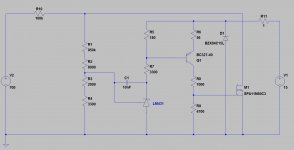
VSS regulator before as above. We note in particular the cascode device Qscm1 with 245V VCS and a spacing between footprint pads of 0.48mm. Also, spacing around unregulated supply input (230Veff AC nom).
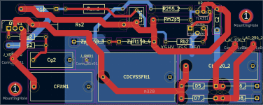
VSS regulator after, below. The supply filter caps and the cascode device are the locations of real voltage differences. Around the output device, all the voltages are roughly the same (320V, 250V, 255V), but peak supply voltage is close to 400V and appears on the filter caps and 245V appears on adjacent pads on the cascode device. I modified the cascode device footprint to bring the spacing up to more than 1.25mm, while leaving the output device footprint alone. The other thing I did was to increase the specified spacing in the PCB software (using net classes) so as to make cut-outs in the ground plane larger, for instance. By setting the spacing in the PCB setup to a safe value, I get a lot of DRC failures, mainly around device pads. These failures are then resolved, or not, on a case by case basis.
On the amp PCB, I will modify both cascode and output device footprint (in both cases, the middle pin is the one with the voltage difference). Modifying the footprint means bending the device leads when mounting, but I think I can manage.
Be careful out there!
Jens
Hesener mentioned high voltage and component clearance. I did have track spacing on my list of things to worry about, and finally got 'round to beginning to inform myself.
Good thing, too. Really helpful links include a calculator: pcbtracespacing and a discussion on KiCAD forum: trace-separation which does mention that it's unknown how device manufacturers expect safe equipment to be built which comes close to 800V / 1000V voltage difference across pins of a device in a TO-220 package.
VSS regulator before as above. We note in particular the cascode device Qscm1 with 245V VCS and a spacing between footprint pads of 0.48mm. Also, spacing around unregulated supply input (230Veff AC nom).
VSS regulator after, below. The supply filter caps and the cascode device are the locations of real voltage differences. Around the output device, all the voltages are roughly the same (320V, 250V, 255V), but peak supply voltage is close to 400V and appears on the filter caps and 245V appears on adjacent pads on the cascode device. I modified the cascode device footprint to bring the spacing up to more than 1.25mm, while leaving the output device footprint alone. The other thing I did was to increase the specified spacing in the PCB software (using net classes) so as to make cut-outs in the ground plane larger, for instance. By setting the spacing in the PCB setup to a safe value, I get a lot of DRC failures, mainly around device pads. These failures are then resolved, or not, on a case by case basis.
On the amp PCB, I will modify both cascode and output device footprint (in both cases, the middle pin is the one with the voltage difference). Modifying the footprint means bending the device leads when mounting, but I think I can manage.
Be careful out there!
Jens
Attachments
Last edited:
- Home
- Amplifiers
- Pass Labs
- X5HV - the F5 principle applied to a headphone amp