Make some simulation in Spice for yourself, rather than just copy what we did.
It is part of the fun.
Patrick
It is part of the fun.
Patrick
Oh, that was the plan all along. I was going to draw everything in LTSpice and get it up and running with models and so on, and then re-run on the big simulator(1) at work so I can get comfortable with it. It just wouldn't feel right to proceed without frowning at DC operating points, linearity and open-loop responses and all that.
Best Regards
Jens
(1) Spectre or HSpice. Absolutely no models for discrete devices, so those will have to be scrounged.
Best Regards
Jens
(1) Spectre or HSpice. Absolutely no models for discrete devices, so those will have to be scrounged.
I am assuming that we need to drive the two inputs in the balanced setup with exactly symmetrical signals. So, if I wanted to have maximum flexibility, should I add a proper single (or switchable single/balanced) input to balanced converter, in the style of the BTSB buffer?
Best Regards
Jens
Best Regards
Jens
If you have a balanced source, you do not want anything else in between.
If you have a single ended source, then you need a SE->BAL converter.
Check this out :
https://www.diyaudio.com/community/threads/necx-and-nesx-single-ended-to-balanced-converters.329767/
Patrick
If you have a single ended source, then you need a SE->BAL converter.
Check this out :
https://www.diyaudio.com/community/threads/necx-and-nesx-single-ended-to-balanced-converters.329767/
Patrick
Nice circuits, for sure.
And I will have to see if I trust the symmetry of the signal I get on the XLR inputs (standalone DAC from NAD).
Best Regards
Jens
And I will have to see if I trust the symmetry of the signal I get on the XLR inputs (standalone DAC from NAD).
Best Regards
Jens
You can always mod the DAC to get perfect balanced out.
Almost all modern-day DACs (other than the ones meant for mobile phones) have balanced out anyway.
So it only depends on the analogue stage.
Best converter is no converter.
Patrick
Almost all modern-day DACs (other than the ones meant for mobile phones) have balanced out anyway.
So it only depends on the analogue stage.
Best converter is no converter.
Patrick
Well, Santa finally got his act together and delivered the cascode and output devices. I had to shop at both RS and Mouser to get 30 P and 30 N MOSFET output transistors, but I got them. Now for a bit of device matching and a lot of simulating.
Best Regards
Jens
Best Regards
Jens
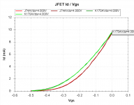
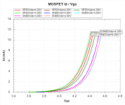
I got the input and output FETs measured on my little device tester / curve tracer(1) and selected a bunch of output devices which were as close as they got. Basically, the high VTH P devices and low VTH N devices were not so dissimilar. My nice little curve tracer cannot do the output devices justice (VDS = 4 produces IDS plots up to about 11 mA and that's it), but I will be operating them at currents which are low compared to their intended use, so the lack of range will hopefully not have a large impact.
The input devices had been bought as matched sets and did indeed match very well. Nice. The J74s have VTH closer to 0 but more gain, and all ID curves meet at VGS = 0 with ID of around 10 mA.
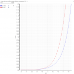
I got the transistor models read into my simulator and fiddled with the parameters to match the measured curves. By adjusting two parameters and using two measurement points I got curves which are representative of how the devices measured. The P50 model using BSIM3v3 worked fine, but the N80C model using different MOSFET models did not produce good results at all. I ended up going with the N50NZ model which turned out to be slightly closer to my measured curves for the N80C parts than the P50 model had been to the measurements of P50 parts. Go figure.
For the JFET models I fitted VTO and BETA model parameters, and for the MOSFET models I fitted VTH model parameter and W instance parameter.
Thanks for the LTSpice input files with all the shiny models 🙂
Pretty pictures: Curve traces for one quad of inputs devices and for four plus four matched output devices. Simulator plots for fitted models.
Next step: Now for actually designing 🙂. The inputs have very similar currents for VGS close to 0, but less similar GM. I think I will end up with source resistors closer to the 10 Ohm of the F5 than to the 50 Ohms, i.e. running in 6 mA - 9 mA range for ID, and maybe a small extra source resistor for the P input type (like shown in this thread). For the outputs, I will try to find source resistors with different values for N and P side, to aim for equal GM and ID at identical voltages across the resistors driven by the currents out of the input cascodes.
Component supply update:
FQP3P50 in stock at RS components, running out of stock at Mouser
For a bit of a change, maybe using Lateral MOSFET outputs (ECX10P20 / ECX10P20 look very suitable) with higher VDS rating output devices as cascodes? The cascode bias generators would have to be something a little firmer than those for the inputs.
(1) DAC75 from Peak Electronic Design
The input devices had been bought as matched sets and did indeed match very well. Nice. The J74s have VTH closer to 0 but more gain, and all ID curves meet at VGS = 0 with ID of around 10 mA.
I got the transistor models read into my simulator and fiddled with the parameters to match the measured curves. By adjusting two parameters and using two measurement points I got curves which are representative of how the devices measured. The P50 model using BSIM3v3 worked fine, but the N80C model using different MOSFET models did not produce good results at all. I ended up going with the N50NZ model which turned out to be slightly closer to my measured curves for the N80C parts than the P50 model had been to the measurements of P50 parts. Go figure.
For the JFET models I fitted VTO and BETA model parameters, and for the MOSFET models I fitted VTH model parameter and W instance parameter.
Thanks for the LTSpice input files with all the shiny models 🙂
Pretty pictures: Curve traces for one quad of inputs devices and for four plus four matched output devices. Simulator plots for fitted models.
Next step: Now for actually designing 🙂. The inputs have very similar currents for VGS close to 0, but less similar GM. I think I will end up with source resistors closer to the 10 Ohm of the F5 than to the 50 Ohms, i.e. running in 6 mA - 9 mA range for ID, and maybe a small extra source resistor for the P input type (like shown in this thread). For the outputs, I will try to find source resistors with different values for N and P side, to aim for equal GM and ID at identical voltages across the resistors driven by the currents out of the input cascodes.
Component supply update:
FQP3P50 in stock at RS components, running out of stock at Mouser
FQP3N80C out of stock at RS components, in stock at mouser
KSC3503DS out of stock at RS components, in stock at Mouser
KSA1381ESTU, in stock at RS components, in stock at Mouser
For a bit of a change, maybe using Lateral MOSFET outputs (ECX10P20 / ECX10P20 look very suitable) with higher VDS rating output devices as cascodes? The cascode bias generators would have to be something a little firmer than those for the inputs.
(1) DAC75 from Peak Electronic Design
Attachments

ECX10P20 / ECX10N20, of course."ECX10P20 / ECX10P20"
200V device for 500V swing ?
Patrick
No, not for 500V swing. Adding a cascode device (on each output, referenced to the supply) would run the actual output device (the 200V max lateral MOSFET) with a fixed VDS - say 25V - and leave the output swing to the cascode device.
This would make the amp look even more like a transductance amp that I would build in an integrated circuit - only not with +/- 0.5 V supply - LOL.
Best Regards
Jens
well, that's fun!
I didn't have to use different degen or gain resistors top and bottom. I did play around with compensation (a lot) and got a fairly friendly looking phase response. No great amount of phase margin, according to lashed-up open-loop response, but very clean looking square waves (and an open-loop rise time of almost 100 kV/s for 35 kV/V open-loop gain).
The open-loop is just connect feedback Rs to gnd (not at output node) and connect a resistor of feedback res half to gnd from out. Then remove input DC offset manually and input 1 mV square wave.
Not done yet, but on the right path.
Best Regards
Jens
Attachments
Very nice! Thats what i was shooting for, 100V/us.well, that's fun!
I didn't have to use different degen or gain resistors top and bottom. I did play around with compensation (a lot) and got a fairly friendly looking phase response. No great amount of phase margin, according to lashed-up open-loop response, but very clean looking square waves (and an open-loop rise time of almost 100 kV/s for 35 kV/V open-loop gain).
The open-loop is just connect feedback Rs to gnd (not at output node) and connect a resistor of feedback res half to gnd from out. Then remove input DC offset manually and input 1 mV square wave.
Not done yet, but on the right path.
Best Regards
Jens
Well, I'm getting closer, but it's not without challenges. The open-loop response I was getting last time was far from the proper OL response. For one thing, I had forgotten to connect the load represented by the feedback network.
I'm settling on 3.5 mA in the inputs, with 50 Ohm degeneration, a lot like the suggestion here (I don't have different degen in P and N inputs). I'm running 1.5 kOhm R on the MOSFET gates and 43 Ohm degen for the MOSFETs. That gives me 24 mA output bias.
I need to set the output bias so it can drive the feedback network in class A for full amplitude, so with a target output of 200 V (amplitude, for each amp,. i.e. half the final bridged amp) that makes a target gain of 200 (my DAC has full output of 2V and if I want 1V of that to produce 200 V amplitude, that's 200 times gain). With the input stage above, that makes the feedback R 11 kOhm. (The open loop gain is 3500, with -3 dB at 5 kHz.)
I design to compensate to just kill ringing on sharp transients. I ended up using both a dummy capcitive load (i.e. permanent load to ground from the output, a very basic Zobel network, if you like), and a cap from MOSFET drain to gain resistor and a cap in parallel with the feedback R. Both of the last caps are discussed by Nelson as optional in his F5 Turbo article. That brings the open loop -3 dB frequency down to 5 kHz (from 20 kHz), but it also avoids some very nasty looking ringing at or above the 5 MHz unity-gain frequency (for closed-loop max swing square wave transient response).
So, I have to trust the transistor models which I most certainly do not, but the caps go in the circuit.
With the compensation like this, the closed-loop -3 dB frequency is 20 kHz, and the feedback at 20 kHz is 13 dB (25 dB at 5 kHz and below) which is not a lot. The linearity appears adequate, with majority H2 distortion at -75 dB for 60 V amplitude at 10 kHz. The H2 would perhaps go down in the final bridged amp.
Question: In Nelson's F5 turbo article, the bias stabilising thermistor is show connected to the drain degen resistor of the output, and in the original article the thermistor is show connected to the positive supply. I missed the bit in between: what is the intention of moving the thermistor, does anyone know?
Best Regards
Jens
Last edited:
Hello again!
Seasonal break allowed a little more time for tinkering; by now, the sizing that I have been working on seems complete, to me.
I went for quite a lot less degeneration for the input devices than proposed previously. The reasoning was that the output device is similar-ish to the original F5 amplifier, so the amount of cap to charge and discharge was not reduced significantly. With the 18 Ohms I chose, I'm getting 5.7 mA in the input devices. The output bias, I set to be able to swing the maximum current and not a lot more; with 10 kOhm feedback resistors, I have 20 mA in the outputs. The MOS devices are biased by 240 Ohm in source degeneration and by resistors from gate to supply (and to source, including thermistor) making some 1.6 kOhm in parallel.
I have added a filter for the input (rolling off below 50 kHz) so as to not run into slew rate limits internally (the current out of the cascodes may not go to zero). I have also added a Miller compensation cap, complete with zero inserting resistor, around the output devices. The bandwidth with the loop opened is just around 20 kHz, and the gain is 1500 times with the loop opened and 400 times with the loop closed.
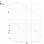
I will add posts about various simulation results later, but here is the LTSpice schematic and the input/cascode output current/output voltage plot for 800 Vppdiff output signal.
Seasonal greetings, and have a great new year's party!
The included LTSpice sheet thingie is My First LTSpice schematic/simulation, and obviously mainly a copy of EUVL's work. Subcircuit terminal currents are saved so as to plot them.
Jens
Seasonal break allowed a little more time for tinkering; by now, the sizing that I have been working on seems complete, to me.
I went for quite a lot less degeneration for the input devices than proposed previously. The reasoning was that the output device is similar-ish to the original F5 amplifier, so the amount of cap to charge and discharge was not reduced significantly. With the 18 Ohms I chose, I'm getting 5.7 mA in the input devices. The output bias, I set to be able to swing the maximum current and not a lot more; with 10 kOhm feedback resistors, I have 20 mA in the outputs. The MOS devices are biased by 240 Ohm in source degeneration and by resistors from gate to supply (and to source, including thermistor) making some 1.6 kOhm in parallel.
I have added a filter for the input (rolling off below 50 kHz) so as to not run into slew rate limits internally (the current out of the cascodes may not go to zero). I have also added a Miller compensation cap, complete with zero inserting resistor, around the output devices. The bandwidth with the loop opened is just around 20 kHz, and the gain is 1500 times with the loop opened and 400 times with the loop closed.
I will add posts about various simulation results later, but here is the LTSpice schematic and the input/cascode output current/output voltage plot for 800 Vppdiff output signal.
Seasonal greetings, and have a great new year's party!
The included LTSpice sheet thingie is My First LTSpice schematic/simulation, and obviously mainly a copy of EUVL's work. Subcircuit terminal currents are saved so as to plot them.
Jens
Attachments
Last edited:

About my simulations: The most important thing in simulation of FET circuits is the transistor models. Unlike bipolars, which by and large all have the same operation, FETs have a confusion of parameters. At work, this is handled by small armies of staff and endless characterisation of test structures. For a hobby project, what we can find in a few minutes of searching is almost as good as it gets. I have attempted to get a little closer to the actual transistor parameters by measuring DC response curves and fitting a couple of parameters (per model) to get the least awful match. This was described in post above . What I am getting at is that some of the characteristics that my simulations depend on (such as everything to do with device capacitances) are of an unknown quality, while at the same time being crucial to simulation of major things like stability. With the DC characteristics (gain, threshold voltages) we are to a certain degree designing out the variability by using local feedback (source degeneration resistors). For the AC characteristics, I might get closer to reality by including explicit capacitances, i.e. I slow down the amplifier to control it. The capacitances I have added should not decrease stability, only bandwidth, so I am pressing ahead.
About the topology: I am following the Nelson Pass article F5 TURBO POWER AMP! This is exceedingly close to the design at the start of this thread (indeed EUVL is credited), with the two following exceptions: Firstly, the thermistor bias stabilisation is included, with the thermistor connected to not the power supply but to the output device source (as far as I can tell, the F5 schematic changed a little). I am planning a series combination of a 4k7 thermistor and a 2k2 plain resistor. I simulated the temperature dependency using a small positive temp co for all resistors except the thermistors which I gave a large (-4% / deg C) negative temp co. The simulation gave a significant lower output bias current for higher temperature, so some sort of self-stabilisation appears to be going on. Secondly, the node between the input FET source degeneration resistors (grounded in a single-ended design) is connected together and otherwise floating - node AC_CMN in my schematic. This was handled slightly differently in the two designs earlier in this thread.
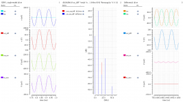
I don't know if it comes from floating the AC_CMN node, but the complete balanced amp does its own single-ended to differential conversion, if called upon to do so. If one input polarity is driven with signal and the other is grounded, we get a small AC voltage on AC_CMN and we get perfectly balanced output signals. While I can understand that this is how it goes for differential pairs, it surprised me that it works equally well for this circuit, but I will happily take the feature. An article series about an amplifier which is similar, but uses bipolar transistors, the CFA of Kevin Gillmore, notes this effect and references commercial designs which use this. I am pleased just to avoid having to make a single-to-diff input stage 😎.
When I say perfectly balanced output signals, that doesn't mean that there is no difference (other than the obvious amplitude difference). The second order harmonic distortion is higher when driven single-ended, but still smaller than the third order HD, so overall the signal quality is more than close enough (THD of -77 dB and -78 dB for 100 Vdiff amplitude) for me.
The included plot shows the time domain waveforms in the two configurations. OUT_CM is the calculated common-mode component and OUT_DIFF is the calculated differential component. As we can see, in both cases only tiny common-mode ripple and a healthy differential signal. The AC_CMN signal is only showing life in the single-ended drive simulation. The middle plot shows the two Fourier transforms of the OUT_DIFF signal. The only difference is that the 2nd harmonic is a little lower. (Yes, I know, it would be nice if the Fourier plot showed markers or something...)
Jens
About the topology: I am following the Nelson Pass article F5 TURBO POWER AMP! This is exceedingly close to the design at the start of this thread (indeed EUVL is credited), with the two following exceptions: Firstly, the thermistor bias stabilisation is included, with the thermistor connected to not the power supply but to the output device source (as far as I can tell, the F5 schematic changed a little). I am planning a series combination of a 4k7 thermistor and a 2k2 plain resistor. I simulated the temperature dependency using a small positive temp co for all resistors except the thermistors which I gave a large (-4% / deg C) negative temp co. The simulation gave a significant lower output bias current for higher temperature, so some sort of self-stabilisation appears to be going on. Secondly, the node between the input FET source degeneration resistors (grounded in a single-ended design) is connected together and otherwise floating - node AC_CMN in my schematic. This was handled slightly differently in the two designs earlier in this thread.
I don't know if it comes from floating the AC_CMN node, but the complete balanced amp does its own single-ended to differential conversion, if called upon to do so. If one input polarity is driven with signal and the other is grounded, we get a small AC voltage on AC_CMN and we get perfectly balanced output signals. While I can understand that this is how it goes for differential pairs, it surprised me that it works equally well for this circuit, but I will happily take the feature. An article series about an amplifier which is similar, but uses bipolar transistors, the CFA of Kevin Gillmore, notes this effect and references commercial designs which use this. I am pleased just to avoid having to make a single-to-diff input stage 😎.
When I say perfectly balanced output signals, that doesn't mean that there is no difference (other than the obvious amplitude difference). The second order harmonic distortion is higher when driven single-ended, but still smaller than the third order HD, so overall the signal quality is more than close enough (THD of -77 dB and -78 dB for 100 Vdiff amplitude) for me.
The included plot shows the time domain waveforms in the two configurations. OUT_CM is the calculated common-mode component and OUT_DIFF is the calculated differential component. As we can see, in both cases only tiny common-mode ripple and a healthy differential signal. The AC_CMN signal is only showing life in the single-ended drive simulation. The middle plot shows the two Fourier transforms of the OUT_DIFF signal. The only difference is that the 2nd harmonic is a little lower. (Yes, I know, it would be nice if the Fourier plot showed markers or something...)
Jens
Attachments
Nice progress Jens! We are looking forward to the measurement results of the build 😀
In single-ended input configuration, you can consider the "other" half a grounded-gate amplifier, driven by the signals at the source pins. and of course, since both P and N are working onto the same output node, it will behave pretty similar to a diff pair.
Guess I have to repair mine soon now, and maybe add a couple of your modifications.....
Hi Hesener,
Thanks. Chewing away at it - the goal for this new years vacation is to have at least the schematic entered into a PCB layout package, if not actually laid out.
More simulations. The capacitors I added slow down the amplifier. While I would normally do an "AC Open Loop" analysis to verify stability, I failed to get it to work for this circuit. A bit of a bummer, that, the simulator has very good facilities for it and I am supposed to know how to drive it to get that answer, but the feedback configuration got the better of me.
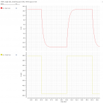
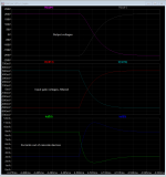
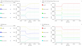
Anyway, the real question should always be: How stable is the circuit in closed loop operation (with correct loads)? And the AC simulation is never the complete answer, because of large signal considerations. Basically, the AC simulation results should be good (phase margin should be within agreed limits etc), but in addition to that, one should always verify that the large-signal operation is correct. A major concern is actual ringing, of course. A second concern is slew rate limitation. Slew rate limitation manifests itself in this amplifier as the input device output current clipping. I have been showing the current out of the cascode for convenience, but it's the same thing. When the current out of the cascode attempts to swing below zero, the loop is opened and there is no such thing as stability - only a hope that settling will be friendly...
So, a large signal transient simulation it is. The 400 Vppampl square wave simulation from above will do very nicely. The schematics I show has the input slowed down and the output device slowed down some more. The end result is a small amount of overshoot on the square wave, but not too much. When, on the other hand, I make a test with no filter on the input and no Miller caps around the output device, I get insanely sharp edges (there's so much bandwidth in the raw devices), amazing amount of overshoot and hard limit of the input device current on one edge. The plot I am showing has good circuit on the left, bad circuit on the right. Observe, if you will, the input device current I_IN_NEG peaks at 28 mA and the output device currents peak at 200 mA. That's a lot of current. Sure, the output slews 800 Vdiff in a microsecond (instead of around 10 microseconds), but I am not needing that kind of response and I would not trust such a fast circuit to be stable... The output voltage (calculated) is OUT_DIFF, the voltage on the gain node GN is AMPN.GN and the output device current is AMPN.I_OUT_N
Best Regards
Jens
Thanks. Chewing away at it - the goal for this new years vacation is to have at least the schematic entered into a PCB layout package, if not actually laid out.
More simulations. The capacitors I added slow down the amplifier. While I would normally do an "AC Open Loop" analysis to verify stability, I failed to get it to work for this circuit. A bit of a bummer, that, the simulator has very good facilities for it and I am supposed to know how to drive it to get that answer, but the feedback configuration got the better of me.
Anyway, the real question should always be: How stable is the circuit in closed loop operation (with correct loads)? And the AC simulation is never the complete answer, because of large signal considerations. Basically, the AC simulation results should be good (phase margin should be within agreed limits etc), but in addition to that, one should always verify that the large-signal operation is correct. A major concern is actual ringing, of course. A second concern is slew rate limitation. Slew rate limitation manifests itself in this amplifier as the input device output current clipping. I have been showing the current out of the cascode for convenience, but it's the same thing. When the current out of the cascode attempts to swing below zero, the loop is opened and there is no such thing as stability - only a hope that settling will be friendly...
So, a large signal transient simulation it is. The 400 Vppampl square wave simulation from above will do very nicely. The schematics I show has the input slowed down and the output device slowed down some more. The end result is a small amount of overshoot on the square wave, but not too much. When, on the other hand, I make a test with no filter on the input and no Miller caps around the output device, I get insanely sharp edges (there's so much bandwidth in the raw devices), amazing amount of overshoot and hard limit of the input device current on one edge. The plot I am showing has good circuit on the left, bad circuit on the right. Observe, if you will, the input device current I_IN_NEG peaks at 28 mA and the output device currents peak at 200 mA. That's a lot of current. Sure, the output slews 800 Vdiff in a microsecond (instead of around 10 microseconds), but I am not needing that kind of response and I would not trust such a fast circuit to be stable... The output voltage (calculated) is OUT_DIFF, the voltage on the gain node GN is AMPN.GN and the output device current is AMPN.I_OUT_N
Best Regards
Jens
Attachments
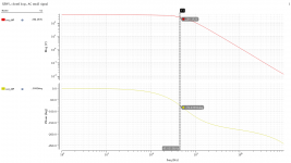
And a nice simple one. The AC response, including the input RC, in closed loop. -3 dB frequency 45 kHz. The input RC cuts in a bit later, so the roll-off we are seeing here is a combination of amplifier roll-off and input filtering roll-off. This can be extended upwards by making the caps smaller, but there is such a thing as too much of a good thing 😉
I went with 400 times gain as a value somewhat below the Stax amplifiers' 1000 times... There will be overall negative feedback, but not a lot (just over 12 dB). Most of the feedback is local, in the source degeneration resistors. This looks simple enough, but more feedback (smaller R21/R22/R23/R24 above) means more current in the output devices means more gain in the output devices means less stability margin. So, again, no such thing as a dimensioning based on small signal considerations.
ETA: The schematric above is slightly wrong. I am using 80 pF input filter cap, not the 160 pF I drew in the schematic above. So, the above is conservative - probably why I got so smooth a transient response. Ooops.
Best Regards
Jens
Attachments
Last edited:
- Home
- Amplifiers
- Pass Labs
- X5HV - the F5 principle applied to a headphone amp