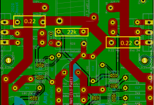
I think that's it -- but should probably let Mooly speak for himself. Am kinda wondering if swapping the ends of the 22k, R7, wouldn't be slightly better still.
The only other notions, so far --
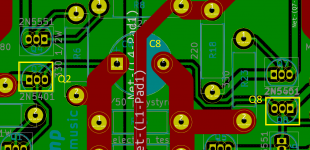
- the VAS Collectors, Q2 and Q8 (the connections to C8) could be narrower traces, which would lower the capacitance to the ground plane; the wide ones for the rails and output lines look good
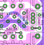
- wondering if the higher power ratings crept into R1 through R6 somehow; a little casual arithmetic shows minimal dissipations -- 90 microWatts for R1, 5-1/2 milliWatts for R2, 11 mW worst case (Q3 Vgs threshold 4V) for R3; 1/4 Watt resistors should be fine for all of them
Keep up the fine work -- this is looking really great!
Cheers
The only other notions, so far --
- the VAS Collectors, Q2 and Q8 (the connections to C8) could be narrower traces, which would lower the capacitance to the ground plane; the wide ones for the rails and output lines look good
- wondering if the higher power ratings crept into R1 through R6 somehow; a little casual arithmetic shows minimal dissipations -- 90 microWatts for R1, 5-1/2 milliWatts for R2, 11 mW worst case (Q3 Vgs threshold 4V) for R3; 1/4 Watt resistors should be fine for all of them
Keep up the fine work -- this is looking really great!
Cheers
Last edited:
Thanks a lot for your answer. About swapping R7's ends, I did swap the ends to how it is on the image, I did that to make the R7 pin touch halfway between the two 0.22 resistors, did think that it would give a better "reading" then if one R7 pin were near one 0.22 and fare from the other 0.22. I may be wrong, but that's the reason for placing the R7 pin there. 🙂
About Q2 I had for some strange reason switched it's name out with the Q4 but do still think you did talk about the Q2 when you did write Q2. 🙂 I have tried to make new traces from both Q2 and Q8 to the C8 and avoided that the traces did go to much under the top side trace.
Your last comment about R1 and power ratings, do I have to admit I do not understand but just a wild guess make me tell you that every resistor, except the special one, are 1W resistors.
Attachments
Last edited:
I hope I have understand it correct, here are my first try out of ? 🙂
look at example here. I tried to show on your layout.
Attachments

Oh thanks, what a great way to do it! 🙂
Just a question, beneath the trace you draws, there are a green trace and they may follow eachother and create an capacitor?
Just a question, beneath the trace you draws, there are a green trace and they may follow eachother and create an capacitor?
Attachments

Last edited:
Yes that is a possibility I haven thought about, but how much will it be if the pcb is screwed to the cabinet and the same are both heat sinks?
so wire from pcb to each leg on the mosfet and in that way avoid any stress?
Sorry but bending tool, is that not just a normal needle nose plier?
Sorry but bending tool, is that not just a normal needle nose plier?
Oh thanks, what a great way to do it! 🙂
Just a question, beneath the trace you draws, there are a green trace and they may follow eachother and create an capacitor?
try crossing at 90 deg if possible. another way is use thicker PCB material
Oh thanks, what a great way to do it! 🙂
Just a question, beneath the trace you draws, there are a green trace and they may follow eachother and create an capacitor?
That is not the way I have shown it.
take the feedback trace from the inductor's pad!
Think of it as a concoction that is still mixing together. You drink the portion that's completely mixed and uniform
Last edited:
okay, so 2 mm instead of 1.6 mm? (or even thicker?)
or try to keep some distance between them so that they are not "one above the other" . 2mm or 2.4 mm would be nice and also sturdy PCB but cost will be higher. so modifying the design is better.
Prasi I have tried to make it better, the reason for the extra green trace is this comment Worst PCB track-layout ever? from Rick PA Stadel.
Attachments
Rotating 90° the resistor with green track and parallel to R18?
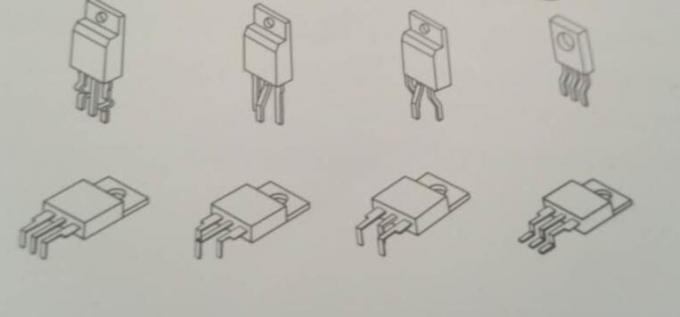
If you´re a plier virtuoso no problem (transistor left top on the three legs).
JP
If you´re a plier virtuoso no problem (transistor left top on the three legs).
JP
Your idea on rotating the resistor is interesting, but I do not know if it is most important with the resistor in the center of the two 0.22 or if a shorter green trace is.
Yes it is maybe not easy to bend the legs like that, but what plier do you think of, being good at that?
Yes it is maybe not easy to bend the legs like that, but what plier do you think of, being good at that?
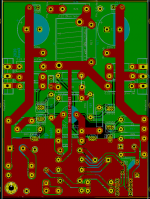
I don't know if this is a good or bad idea. The schematic has two grounds a normal ground and a "clean ground" I have now split them up instead as before where I had them combined.
I have done it by making a filled zone on the front. The front-zone do only cover the lower 1/4 of the board.
I have done it by making a filled zone on the front. The front-zone do only cover the lower 1/4 of the board.
Attachments
Power supply for Mooly?
Since I have already started this thread and the subject is still the Mooly amp, I thought why not keep using this thread, instead of starting a now.
Please say if you think I it's better to start up a new thread! 🙂
First do I have to say that Mooly has provided me with a drawing of a simply power supply that works for his amplifier, and thanks to him for that!
When that is said, I think it's more fun to experiment and may learn me more.
Therefore have I tried to make a circuit that, do I hope, kills noise and ripples, it's not regulated but it can be but I have not found anyone using a regulated power supply. There has to be a reason for that?
Q1 and Q6 are propperly wrong, but I can not decide where to place N or P type mosfets. Also R3 is propperly wrong, but I can not find out how to handle the two inducters "kick back" to zero when turning off.
The caps on the bridge rectifier is to suppress Voltage overshoot while switching.
Schematic below, hope you'll take a look 🙂
Attachments
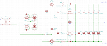
D1 and D2 are the wrong way around and I'm not sure the tant is a great idea either tbh 🙂
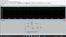
Ripple filters can work OK but also add to losses in the supply due to voltage dropped across them. Look at Vin and Vout here for a 1 amp (ish) load. The filtering is good but the losses high.
Edit... the FET bridge is another story.
Ripple filters can work OK but also add to losses in the supply due to voltage dropped across them. Look at Vin and Vout here for a 1 amp (ish) load. The filtering is good but the losses high.
Edit... the FET bridge is another story.
Attachments
- Home
- Design & Build
- Construction Tips
- Worst PCB track-layout ever?