It's in Kicad right ? Could you please make a simple printscreen, I don't have Kicad installed right now ?
Ok, so now I'm really lost. The layout in post 82 seems to match that schematic, in terms of positions and size of most parts. But the layout in posts 89 or 99 don't make any sense. 😕
As an example, let's take r25-r26. They are small resistors in post 82 but are now big ones in post 89/99 ? And why are they near the mosfets ?
As an example, let's take r25-r26. They are small resistors in post 82 but are now big ones in post 89/99 ? And why are they near the mosfets ?
Maybe this can help, but first, I am not sure I do completely understand.
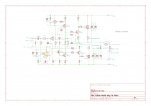
I did to a start, draw the schematic and Mooly was so very kind to check it for errors and he found one error.
After that did I chose some components and did try to make a layout. I was advised to select some smaller components and try again.
Any reason for any placement, is almost alone from me guessing what is what on your great layout. 🙂
Ok... to go forward, I would suggest you to establish a simple bill of material (BOM). Simply:
C5 - 10uF/25VDC - electrolytic cap - 2mm/5mm (lead spacing/diam)
R11 - 22K - 0.6W metal film resistor - 6.3mm/2.4mm (length/diam)
C13 - 100nF/100VDC- MKT cap - 5mm/2.5mm/7.2mm (lead spacing/width/length)
and so on. Then we will check together if all these make sense with regard to the schematic. Then you will be able to complete your schematic with the correct footprint for each part. Then only can you start the layout.
PCB doesn't match schematics, as I see.
There are several mistakes.
For example, C13 has to be a film cap near the opamp. Or no?
C9-D1: where is C9?
C1-R1: where is C1?
Something strange with R8 on the PCB.
And so on.
There are several mistakes.
For example, C13 has to be a film cap near the opamp. Or no?
C9-D1: where is C9?
C1-R1: where is C1?
Something strange with R8 on the PCB.
And so on.
Last edited:
Sorry for my very slow answer but I havn't been home, I'll try to make a BOM, I have tried to ask KiCad to do it, but all I get is some strange and unusable XML files.
VovK Z Thank you so much for checking for error!! You are right, but it's my fault, when trying to draw 00940's layout, did I ask KiCad to rename several components, to mach the drawing better. Here is the correct document.
I am looking for a cermet (ceramic metal) non-inductive THT 5W resistor but I can't seem to fine one. Any idea where to find some? (DigiKey and Mouser do not show any).
Attachments
I like TR50 from Hitano. Non-Inductive design, take a small place, 3W at free air, good TCR.I am looking for a cermet (ceramic metal) non-inductive THT 5W resistor but I can't seem to fine one. Any idea where to find some? (DigiKey and Mouser do not show any).
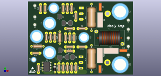
So pew, what a task and what fun!!
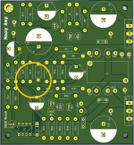
I have now ended up with a pcb I think is fine🙂
The BOM is still under writing.
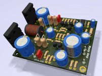
I have now ended up with a pcb I think is fine🙂
The BOM is still under writing.
Attachments
Last edited:
Okay thanks, I did avoid that because I thought they would be bad.
My "logic" was build on the advice that I should use as wide tracks as possible. But when I did look at the pads with thermal reliefs, there were about no track left that did connect to the pads. 🙂
My "logic" was build on the advice that I should use as wide tracks as possible. But when I did look at the pads with thermal reliefs, there were about no track left that did connect to the pads. 🙂
You can safely use thermal relief on pads connected to copper pours. It will not lead to problems since the length of the spokes connecting the pad with the copper pour is too short to have appreciable inductance and resistance.
I recommend using thermal relief on all GND pads otherwise soldering them will be very difficult.
Wise; but really essential for dip soldering, less so for hand soldering which is probably what FM will do. In hand soldering the worker can observe the joint heat and solder flow. Dip-solder, all joints get just-enough heat and any change in the process means big pads will be under-heated.
PRR i am planning on hand soldering, as you say🙂
I am using one of Hakkos soldering stations.
The question is what size pad would be best if the leads max thickness is 0.8 mm?
I am using one of Hakkos soldering stations.
The question is what size pad would be best if the leads max thickness is 0.8 mm?
Major error?
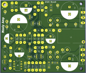
I have just found out I may have an giant error in my PCB!
00940 did kindly share his fantastic layout and I did try to do my best to "steel" it, but it looks like I have made a huge error while trying to copy it.
I did use the KiCad schematic as foundation for my try, but as you can see in the orange circle, do 00940's layout (red and blue) have two resistors go in parallel, while in my try, do they not connect.
Attachments
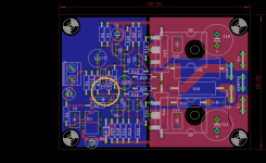

How can that be, does the app not give an error or show an 'unconnected' list? Have you enabled DRC? Did you really use the same schematics?
Jan
Jan
- Home
- Design & Build
- Construction Tips
- Worst PCB track-layout ever?