Hi
It's why for a low Z transformer like for 6C33, 6336, 6AS7.... you can winding it with bifilar technic
Yan
It's why for a low Z transformer like for 6C33, 6336, 6AS7.... you can winding it with bifilar technic
Yan
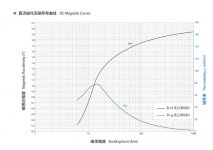
I collected some datasheet of silicon iron back from 1970's to 2016. Few of them have a detial about AC permeability in low-intensity magnetic field. They always offer a DC permeability VS exciting force.My Vacuumschmelze databook is full of those permeability curves. I have also data from other manufacturers from all over the world. It’s not so rare as you say. But skip the EI cores.
At AC power source, there are two kind of permeability. Elastic and viscous permeability. I never find any specification give that graph.
Attachments

Think of capacitance as dependent from alternating voltage potential difference. Primary voltage swing is highest at the anode (makes sense), while it is ideally 0 where the DC power supply, shunted by the decoupling capacitor. An regular tube amp OPT has a high ratio impedance transformer, for example a 3,5k\8R transformer has ~21:1 turn ratio. That means, if you have 210V AC on the anode, you will have 10V max secondary voltage. In practice this secondary voltage is too small to be of practical used, so Patrick for simplicity sake assumed the whole secondary winding would be considered as 0 DC potential.
In Patrick Turner's interleaving schematic depicted, the P/S capacitance will be the highest at the first primary (Anode) layer an the AB CD secondary layer.
In this layer the capacitance factor Cf = (12,5/13)^2 * Cst. Cst stands for static capacitance, the equivalent of a parallel plate capacitor. The 13 is the number of primary layers in Turner's interleaving schematic, and 12,5 stands for the current layer number with 0,5 subtracted for an averaging midpoint.
On the other hand at the top B+ primary and MN OP secondary layer, +, Cf = (0,5/13)^2 *Cst. You then realize it's 625 times less than the anode counterpart. Capacitance decays proportionally to impedance, from Anode to B+.
Patrick used layer numbers from a simplistic point of view of believe. You can use voltages or even impedance decay if you want. In another great book called "Transformers for Electronic circuits" by Nathan R. Grossner, the formula quoted used voltages.
For a 1:1 interstage transformer for example, by winding bifiliar you get zero capacitance between the primary and secondary due to the fact the voltage gradient is equal between wires. Of course if you reverse a polarity, you will get a 100% shunt capacitance effect because of voltages between windings in antiphase. So the benefits are extremely low amounts of leakage inductance with no primary to secondary capacitance = easiest HF bandwidth as hell.
In practice, you will still get some pF of clumped primary, clumped secondary and secondary primary to core capacitance.
In Patrick Turner's interleaving schematic depicted, the P/S capacitance will be the highest at the first primary (Anode) layer an the AB CD secondary layer.
In this layer the capacitance factor Cf = (12,5/13)^2 * Cst. Cst stands for static capacitance, the equivalent of a parallel plate capacitor. The 13 is the number of primary layers in Turner's interleaving schematic, and 12,5 stands for the current layer number with 0,5 subtracted for an averaging midpoint.
On the other hand at the top B+ primary and MN OP secondary layer, +, Cf = (0,5/13)^2 *Cst. You then realize it's 625 times less than the anode counterpart. Capacitance decays proportionally to impedance, from Anode to B+.
Patrick used layer numbers from a simplistic point of view of believe. You can use voltages or even impedance decay if you want. In another great book called "Transformers for Electronic circuits" by Nathan R. Grossner, the formula quoted used voltages.
What's the benefit of bifilarly wound output transformers? Winding the primaries bifilarly only makes sense in unity coupled designs, otherwise intra winding capacitances will be increased dramatically.
Best regards!
For a 1:1 interstage transformer for example, by winding bifiliar you get zero capacitance between the primary and secondary due to the fact the voltage gradient is equal between wires. Of course if you reverse a polarity, you will get a 100% shunt capacitance effect because of voltages between windings in antiphase. So the benefits are extremely low amounts of leakage inductance with no primary to secondary capacitance = easiest HF bandwidth as hell.
In practice, you will still get some pF of clumped primary, clumped secondary and secondary primary to core capacitance.
Nice graph, those curves can be easely found from several manufactures online.I collected some datasheet of silicon iron back from 1970's to 2016. Few of them have a detial about AC permeability in low-intensity magnetic field. They always offer a DC permeability VS exciting force.
At AC power source, there are two kind of permeability. Elastic and viscous permeability. I never find any specification give that graph.
Thank you very much! It's quite a while since I had read Mr. Turner's article. I need read them again.Think of capacitance as dependent from alternating voltage potential difference. Primary voltage swing is highest at the anode (makes sense), while it is ideally 0 where the DC power supply, shunted by the decoupling capacitor. An regular tube amp OPT has a high ratio impedance transformer, for example a 3,5k\8R transformer has ~21:1 turn ratio. That means, if you have 210V AC on the anode, you will have 10V max secondary voltage. In practice this secondary voltage is too small to be of practical used, so Patrick for simplicity sake assumed the whole secondary winding would be considered as 0 DC potential.
In Patrick Turner's interleaving schematic depicted, the P/S capacitance will be the highest at the first primary (Anode) layer an the AB CD secondary layer.
In this layer the capacitance factor Cf = (12,5/13)^2 * Cst. Cst stands for static capacitance, the equivalent of a parallel plate capacitor. The 13 is the number of primary layers in Turner's interleaving schematic, and 12,5 stands for the current layer number with 0,5 subtracted for an averaging midpoint.
On the other hand at the top B+ primary and MN OP secondary layer, +, Cf = (0,5/13)^2 *Cst. You then realize it's 625 times less than the anode counterpart. Capacitance decays proportionally to impedance, from Anode to B+.
Patrick used layer numbers from a simplistic point of view of believe. You can use voltages or even impedance decay if you want. In another great book called "Transformers for Electronic circuits" by Nathan R. Grossner, the formula quoted used voltages.
Thanks again.
This is the way to go 🙂Vacuumschmelze
Check EI laminations with double sized window.
That is not very useful, I have to build a test circuit by myself to get what I need.Nice graph, those curves can be easely found from several manufactures online.
Isn't this discussion in general, and wasn't my detailled question about output transformers?For a 1:1 interstage transformer for example...
Best regards!
Ah yes, my bad!
Winding bifiliar step-down transformers will results in lots of capacitance indeed.
Personally I don't believe bifiliar winding of an output transformer is really necessary, even for unity coupled designs. I suspect it might have something to do with ease of production.
Winding bifiliar step-down transformers will results in lots of capacitance indeed.
Personally I don't believe bifiliar winding of an output transformer is really necessary, even for unity coupled designs. I suspect it might have something to do with ease of production.
McIntosh's MC-3500/MI-350 output transformers even feature pentafilarly wound primaries. I doubt they did it for ease of production.
Best regards!
Best regards!
I guess, but am not sure of course, McIntosh used two different wire gauges in these OT's: Bigger diameters for the plate and cathode sections, smaller dias for the screen, bootstrap and feedback sections. Or they used the same dia/cross section and paralleled multiple wires for the plate and cathode parts.
Best regards!
Best regards!
I know a company in Germany who probably can do make such combi wires. They make all kinds of weird wiresI guess, but am not sure of course, McIntosh used two different wire gauges in these OT's: Bigger diameters for the plate and cathode sections, smaller dias for the screen, bootstrap and feedback sections. Or they used the same dia/cross section and paralleled multiple wires for the plate and cathode parts.
Best regards!
https://www.packlitzwire.com/Who's it? Mind to share, please?
Best regards!
They can make many more then what you see on the website. I have bifilar twisted wire from them for example, I also saw silverwire in the past on their website.
Hi 50AE,In Patrick Turner's interleaving schematic depicted, the P/S capacitance will be the highest at the first primary (Anode) layer an the AB CD secondary layer.
In this layer the capacitance factor Cf = (12,5/13)^2 * Cst. Cst stands for static capacitance, the equivalent of a parallel plate capacitor. The 13 is the number of primary layers in Turner's interleaving schematic, and 12,5 stands for the current layer number with 0,5 subtracted for an averaging midpoint.
On the other hand at the top B+ primary and MN OP secondary layer, +, Cf = (0,5/13)^2 *Cst. You then realize it's 625 times less than the anode counterpart. Capacitance decays proportionally to impedance, from Anode to B+.
Patrick used layer numbers from a simplistic point of view of believe. You can use voltages or even impedance decay if you want. In another great book called "Transformers for Electronic circuits" by Nathan R. Grossner, the formula quoted used voltages.
If we removed the secondary layer closest to primary Point 1, we can highly reduce the capacitance. But what the biggest fault? A greater leakage inducutance?
Best regards!
Andy
Attachments
Yes. You will get a point with higher leakage. But in a situation such as this one, you might get a more beneficiary ratio Cs for Ls tradeoff. On the other hand, it would be a dumb thing to do it at the top where the B+ is, because you would get the higher leakage with no practical reduction of capacitance.
The key for making good identifying transformers is to identify which flaw can become a benefit. For example you could use the outer secondary layer for
Once you start calculating capacitance your imagination can soar. But beware, you need some failed projects to identify how capacitance distribution affects all varieties of transformer geometries.
Take a look of RDH4 and N. Crowhurst papers as well. There are asymmetrical types of interleaving, such as P3-SS-P6-S. It's a benefit to start at the bottom P3 end as anode.
Take a look at these two transformers. They have the exact same interleaving. S3-P22-S3. But differently dumped capacitances around. Notice the doubling of frequency in the dipping resonance. The transformers have a calculated 75mH of leakage inductance, Patrick's formula used.
Attachments
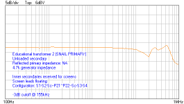
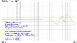
Impressive! Anyway, what's the difference between both configs? I just can't get the abbreviations sorted...
Best regards!
Best regards!
In this case,
would it have been better to make a
P s P K s P K s P instead of s P s K P K s P s
differentiate the thickness of the insulation (for exemple) 0.8 anode side to 0.3 +HT side, between P and S and 0.2 between K and S
I created an Excel page to calculate and balance the capacity of each interface.
50AE
You said that résistance of each S must be équal.
What's happen when some of S are in parallel strapping for 4 or 8 for exemple and all of them are employed
Yan
- Home
- Amplifiers
- Tubes / Valves
- Winding my own output transformers...dumb idea?