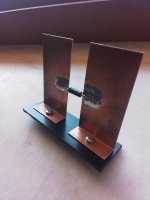
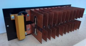
And think the arrangement from #177 is a winner. With 70-72 mA the zenner didn't heat more than 55C (131F). 31.5V over zener, meant 2.27W but at 55 degree is not excessive hot. I even can keep the finger on the case for seconds...The diode derate with 1.5V with summed errors 1.5x12 = 18V but copper mass have enough thermal inertia to keep it thermic steady over power transients so I think even derated voltage will be steady with musical signal so can be considered like a 31.5V diode. Of course if the screens will draw max currents for long period that will cool down the diodes and will clamp 18V down. But on the power transients I don't think will be the case. Thanks very much all of You gents for support.
Late: carefully measures should be taken when short soldering on high copper mass still.
Late: carefully measures should be taken when short soldering on high copper mass still.
For the thick pcb 3 oz - 0.0105 mm double sided not works as well as individual heatsinks. At same 2 square inch for each end (one inch per pcb side x2) I used, I ended with almost 90*C instead 50*C with 0.5 mm thick heatsinks. I.m sure it will work better with 4 square inch per side as You said but that's excessive large for my app please. All temps measured at the end of the case.2W from natural convection would probably put Tj at the 200C Si limit. The case could be hot enough to burn flesh. If you were only using ONE, and it was mounted to a .062 FR4 with 4 square inches of 2 oz Cu on each end it might be good for a couple watts reliably. That would be a typical power supply application. They can also tolerate much higher non repetitive surge currents than one watters, in applications where they suppress transients.
I don’t think they had tube amp shunt regulators in mind when they made these.
Last edited:
Heatsinking is trying to use low thermal resistance paths to ambient air temp. You can attempt to do that with one interposing item of metal, like post #182, which provides a low thermal resistance from the device junction to a large surface area for convection cooling into local ambient air. The inconvenient aspect of that layout is that you then have to physically mount multiple such units and electrically link them all.
In post #142 you started with all devices on a convenient single board, that could be more easily mounted and linked. However that board needed to be enhanced with added fins, and a way of lowering the thermal resistance from each device to a local fin (ie. not by a significantly long lead length). One option would be to solder a fin to each pcb section, and to simplify retrofitting without repositioning each zener, the fin could be also soldered directly to the zener lead where it exists its package. Each zener could remain as shown, or repositioned to sit on the pcb and use the pcb land as the close metal heat spreader.
A one-to-one comparison would use fins of the same surface area for both #142 and #182.
A typical rule of thumb for silicon devices is to try and keep Tj below about 100-110C, as that allows some margin against poorer ambient air flow or short duration increase in device dissipation. You can try and estimate Tj be measuring a spot temperature close to a device, but be mindful that the junction would be somewhat hotter than the measured temp, and the probing of the temp may be wicking away heat, or otherwise have inaccuracies.
Last edited:
Thanks. Was more like that. Same area taking in consideration the both sides. But half air exposed surface.
That.s interesting- in the same way efficiency convection was loose in the case the heatsink was folded in 'U' shape. It makes the inner face of ''U' less effective, despite the fact almost 3/8 was in between. The difference was 10*C more than 'L' shape for the same heatsink.Than the spacing between fins becomes a problem. Minimal room should be preserved to keep the same heatsink efficiency for a determined air flow (natural in this case).
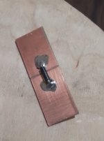
That.s interesting- in the same way efficiency convection was loose in the case the heatsink was folded in 'U' shape. It makes the inner face of ''U' less effective, despite the fact almost 3/8 was in between. The difference was 10*C more than 'L' shape for the same heatsink.Than the spacing between fins becomes a problem. Minimal room should be preserved to keep the same heatsink efficiency for a determined air flow (natural in this case).

Last edited:
Now, a safety measure question please.: The regulator will hang exposed out of chassis. I Intend to protect the hardware under voltage with a metalic mesh cage. That is rigid enough to prevent accidentally touch. Still just in case of shock deformation of the mesh... or some making the high voltage contact possible between heatsink under voltage and mesh cage I ask if a fused protection of circuit and a hard wiring of the metalic mesh directly to the earthing nut may be just enough please ? Thanks.
Last edited:
Last edited:
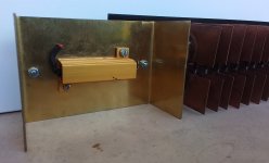
You seem to have copper sheet around - perhaps do the same heatsinking for the metal housed resistor ?
With 100 square cm brass plate sink the temperature was going to half: 50*C please. ...but have only 6.5W dissipated with actual voltage of the mains, current 63 mA around
Last edited:
That's now a lot of hardware to generate a rail that is lower than your main B+ level. Perhaps may have been simpler and easier to just use a choke input filtered rail from the same secondary HT, as the current through the choke filtered rail is fairly low, and you would likely end up with a lower ripple voltage than your zener dropped situation, and far less power dissipated.
Thank you. I can even make a secondary winding on the same core or modify the existing one to be stacked as well but the ideea was to confront with a medium current 100mA zener shunt regulator because as elegant simple it is, seems extremely provoking to build even for such small currents. 40w dissipation for 100mA looks ridiculous I know.Thanks.
Last edited:
There wouldn’t be as much pretty copper metal work in a solution with less dissipation. it’s going to be a unique amplifier…..
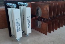
I tested also this one: 2 pcs 2.2k / 10w in parallel. For 9w dissipation, meant 4.5w each the resistors case got 90C degree.
View attachment 1328451
The soldering it took to mount those rectifiers to the heat sink fins wasn't your normal standard quick heat, apply to flow, and then get off the SS device. That took a lot of above normal heating time to attach those with that smooth soldering along the entire lead length. I'd be afraid of overheat damage showing up if those rectifiers are carrying anything near their rating. Why such an overkill on the heatsinking if the rectifiers are not carrying current over sensible dissipation needs?
I already mentioned somewhere carefully soldering required. That do not mean is complicated at all: a good 60W iron, a surgical tweezer used as thermal shunt and a wet cloth 'thimble' on a finger keeped like a wet sponge over capsule. Pre-tined and a pre-heating is a prerequisite
The dissipation needs to be exactly what the screens draw to keep the voltage stable. My screen grids dissipate the same power at max output. 75mA around at 360V. So will be supplied constantly at 360V no matter how much the screens current draw...more or less, this regulator being derated by input voltage aso. But my tests shows around 5 percent which I consider pretty acceptable.
The unit get 40w around, the screens dissipate 30w at max power (5w per tube x 6 pcs) but will be external mounted in back of chassis. I am not concerned by global warming at all , my care was to ensure stable conditions of circuit. As much as I know a regulator should be designed for the max current the load it need. Am I wrong please ?
Last edited:
I think the approach of using zenner diodes is wrong, they are sensitive when they heat up, there are other alternative solutions, have you thought about them?
Not at all. Of course is wrong... That's the reason the topic was rolled for over two weeks. I.m not familiar with silicon devices and did not imagine a 5w device is usable just for half of watt or so. Fortunately we find a solution to make it usable for almost 3W dissipation with natural cooling but is a unusual one. It looks like a tank but my zeners runs at 2.5 -3w dissipation at 50*C with a minimal thermal derive and the regulation works within 5 percent. The Zener I used are max rated at 160mA. I asked for half, make it usable for 80mA I draw. There is no way to use this zener for 80mA without unusual sinks. Mostly use it for 10-20 mA around. For 10-20mA are suited 1W devices I think...Those 5w was claimed to be operational within 160mA, you need to assure conditions to that. But the power is power, 40w dissipation request the same heatsink size no mater if diodes, transistors or whatever is used, cannot be make it smaller than that. A lot of valuable solution and suggestions was offered here and finally was done. Is powered for hours and work without a problem.Thank You.
Last edited:
- Home
- Amplifiers
- Tubes / Valves
- Williamson first stage question
