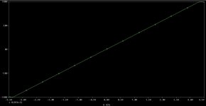
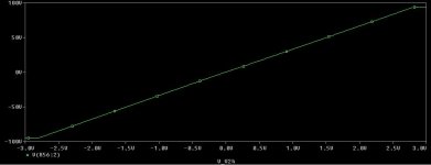
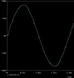
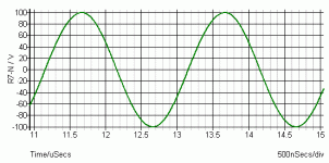
500 kHz attached.
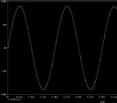
Have you verified the distortion level? It does not look to me as if the waveform you show would have less than 3% distortion.
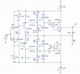
I spiced a CFA with complementary output.
OK, but I think there are several issues which should be resolved before you try this in real world. However, before I waist more time in this thread, I want to make sure that my contribution is actually of interest for you. Have you looked at the amplifier schematic I posted, and do you have particular, verified reasons why you think that your version is any better?
Samuel
Sir,
I am 100% sure that your schematic must be way better than mine (I am really bad in linear design). I am restricted by component count and size. I dont claim any superiority over your schematic.
And the schematic I posted used 2n3904/3906 models and is only a tentative one. Even 510pF is too big. I know that it looks doubtful, artificial etc etc.
I have another using exactly 2SA1407/2SC3601 models, same mosfets. THD is 0.5% at full power (500kHz), gate stopper 10R and comp n/w is 100R/100pF. Again, all this is only SPICE, I accept it.
I have seen your schematic and it is really nice and professional, especially the VAS. But I would like to have a simple, small circuit.
Last edited:
Complexity is a perfectly valid reason--we just have to know it! I'm not sure though if it is indeed realistic to achieve the performance you want at much lower complexity; this is not a trivial task.
The main difficulty with your approach is the large dependence of output stage quiescent current on MOSFET threshold voltage. In SPICE world you can adjust things until everything is biased just as we want, but this does not mean that the bias points will be the same when we build the circuit. This applies particularly as complementary devices are involved, and their match influences the DC offset of the amplifier. To easily reproduce this in simulation you can put a DC source in series with the gate of one MOSFET, and apply some hundred mV to simulate threshold voltage variations. Check how much the output stage bias current, and amplifier offset, varies.
To mitigate these effects it is possible to use a quiescent current control system. There are various approaches here, but none is truly simple. For a one-off build you can select R1 and R4 to get both low offset, and the desired quiescent current. I'm not sure if there are any significant effects on THD when these resistors don't match; if so, you'd need to match M1/M2 for Vgs at the desired quiescent current.
Then we could replace the output transistors with BJTs; their Vbe characteristics is much more dependable. The problem here is their reduced safe operating area (SOA); I'm not sure if any device exists which simultaneously has sufficient SOA and speed.
The problem here is that the Miller compensation capacitors should connect to the collectors of Q3 and Q4 respectively (rather than the gates of M1 and M2). Then a value in the pF range will suffice.
However, the Miller compensation loop might then become instable, as the emitter followers Q5-Q8 are not well biased. These transistors definitely need a bit of quiescent current to work well--say 100 uA, better 1 mA. Use two small-signal diodes between their bases, and small emitter resistors.
There's more to say, but I think it's most easy if you apply these changes, and then report back.
Samuel
The main difficulty with your approach is the large dependence of output stage quiescent current on MOSFET threshold voltage. In SPICE world you can adjust things until everything is biased just as we want, but this does not mean that the bias points will be the same when we build the circuit. This applies particularly as complementary devices are involved, and their match influences the DC offset of the amplifier. To easily reproduce this in simulation you can put a DC source in series with the gate of one MOSFET, and apply some hundred mV to simulate threshold voltage variations. Check how much the output stage bias current, and amplifier offset, varies.
To mitigate these effects it is possible to use a quiescent current control system. There are various approaches here, but none is truly simple. For a one-off build you can select R1 and R4 to get both low offset, and the desired quiescent current. I'm not sure if there are any significant effects on THD when these resistors don't match; if so, you'd need to match M1/M2 for Vgs at the desired quiescent current.
Then we could replace the output transistors with BJTs; their Vbe characteristics is much more dependable. The problem here is their reduced safe operating area (SOA); I'm not sure if any device exists which simultaneously has sufficient SOA and speed.
Even 510 pF is too big.
The problem here is that the Miller compensation capacitors should connect to the collectors of Q3 and Q4 respectively (rather than the gates of M1 and M2). Then a value in the pF range will suffice.
However, the Miller compensation loop might then become instable, as the emitter followers Q5-Q8 are not well biased. These transistors definitely need a bit of quiescent current to work well--say 100 uA, better 1 mA. Use two small-signal diodes between their bases, and small emitter resistors.
There's more to say, but I think it's most easy if you apply these changes, and then report back.
Samuel
...For the time being the load is 1k resistive.
by not responding to repeated requests for more signal, load details you are wasting the efforts of people willing to help you
a amp circuit is not designed "for the time being" it is designed for a signal and load and sometimes there are no incremental paths from a design appropriate for one set of conditions to one that will work at all under different load conditions - Capacitive load is a particular cause of amplifier instability and should be designed for from the start
designing for signal limitations can save much expense if say you only need ms of pulsed power, or any DC componnet could be supllied by bias
R and AC coupling the amp for >100 KHz ...
Last edited:
X2by not responding to repeated requests for more signal, load details you are wasting the efforts of people willing to help you
a amp circuit is not designed "for the time being" it is designed for a signal and load
I think, people are too kind. I just watch and did not participate in this "riding in a boat". Design with such unclear and moving requirements is non sense or, could be a bad joke..
There's more to say, but I think it's most easy if you apply these changes, and then report back.
Thank you very much. But I dont really follow the idea behind the emitter resistors. ?????
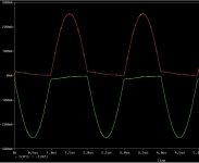
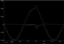
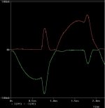
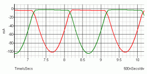
Earlier, the THD was good, but the current waveforms were shooting upto several amperes, although quiescent current was small. I/p current was not equal to O/p current. And, there was ringing at the EF inputs (and hence the gates) as they weren't biased.
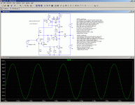
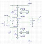
Now that I have made most of the changes you mentioned, these problems have vanished, and I post the most recent version.
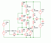
The circuit, output voltage, supply currents, power dissipation and the class AB characteristics. And please read 2SC3601/2SA1407 instead of 2Nxxxx.
Quiescent current is around +/-5mA.
Attachments
Last edited:
Design with such unclear and moving requirements is non sense.
Good specs pay half the rent, no doubt!
Now that I have made most of the changes you mentioned, these problems have vanished, and I post the most recent version.
Better, but we're not quite there yet. As follows:
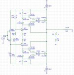
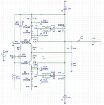
* There is no need to provide extra current sources to bias the emitter followers (Q112 etc.). Just put D3 and D4 between R6 and the collector of Q73 (and similarly for D9/D10).
* The emitter followers (Q112 etc.) need emitter resistors with at least 20 mV, better 100 mV DC drop. Otherwise thermal effects and transistor tolerances will make the quiescent current far too variable.
* There is probably a need for feed-forward capacitors in the emitter followers (Q112 etc.), to keep the Miller compensation loops stable. Put about 100 pF from the collector of Q73 to the gate stopper resistor of M40 (and similarly for the other half).
* As said before, the Miller compensation capacitors C19/C20 need to go to the collector of Q73/Q76. Otherwise stability will be ill-defined.
* The feedback network impedance is way too low. You're waisting more power in the feedback network than in the load! Use something like 10k for the feedback resistor, and scale down the Miller compensation capacitors to about 2.2 pF each.
EF biasing ok. Cannot increase emitter resistor beyond 10R, driver output impedance gets spoilt.
Feedforward and Miller ideas not clear yet
Feedforward and Miller caps to goto collector of Q73 or to between D3&D4?
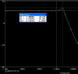
10k feedback resistor makes sine wave asymmetry, 1k works well.
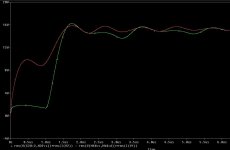
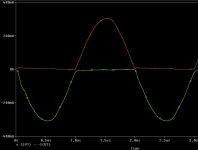
Latest version posted. Current waveform showing small amount of shoot- through.
Feedforward and Miller ideas not clear yet
Feedforward and Miller caps to goto collector of Q73 or to between D3&D4?
10k feedback resistor makes sine wave asymmetry, 1k works well.
Latest version posted. Current waveform showing small amount of shoot- through.
Attachments
Last edited:
The collectors of Q115 and Q124 should definitely be grounded.
There's a chance that the circuit needs gate resistors in the 100 Ohm range anyway, to prevent parasitic oscillation.
Doesn't really matter, I'd take the collector of Q73 for the caps of the upper half, and the collector of Q76 for the lower half.
That's because there is a very large DC current flowing through the inverting input, as a result of the ill-defined bias of the output stage. Let's first get the compensation right, then we'll look into this...
Samuel
Cannot increase emitter resistor beyond 10 Ohm, driver output impedance gets spoilt.
There's a chance that the circuit needs gate resistors in the 100 Ohm range anyway, to prevent parasitic oscillation.
Feedforward and Miller caps to goto collector of Q73 or to between D3 & D4?
Doesn't really matter, I'd take the collector of Q73 for the caps of the upper half, and the collector of Q76 for the lower half.
10k feedback resistor makes sine wave asymmetry, 1k works well.
That's because there is a very large DC current flowing through the inverting input, as a result of the ill-defined bias of the output stage. Let's first get the compensation right, then we'll look into this...
Samuel
Last edited:
The only way to reconcile performance, simplicity and low power is to go circlo:
Here is another example, delivering >100V peak @ >100mA, with only 5 transistors and 10mA quiescent current.
If low capacitance, video-type transistors are substituted for Q3 to Q5, further improvements in performance are even possible.
Here is another example, delivering >100V peak @ >100mA, with only 5 transistors and 10mA quiescent current.
If low capacitance, video-type transistors are substituted for Q3 to Q5, further improvements in performance are even possible.
Attachments
The only way to reconcile performance, simplicity and low power is to go circlo.
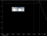
If I'm not mistaken this amp has very high offset, so a bit inconvenient to apply for a DC coupled design. What is the distortion at the intended level, frequency and load?
Miller caps in place.
These are the feed-forward caps, set them to about 100 pF.
One Miller cap goes from drain M48 to collector Q3, and the other from drain M47 to collector Q4.
Samuel
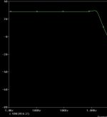
In the case of the sim, the offset is about 1V; in reality, it could be several volt in either direction, and it will be power supply and temperature dependent.If I'm not mistaken this amp has very high offset, so a bit inconvenient to apply for a DC coupled design. What is the distortion at the intended level, frequency and load?
But all depends on the DC accuracy required, and compared to the 200Vpp output, this may (or may not) be acceptable.
Anyway, one more transistor at the input would solve the issue, or alternatively a low frequency op-amp if millivolt accuracy is required. The THD under the conditions shown in the sim is 0.98%.
It is getting better and better!
It is hard to make fast amplifier, unless using much current.
Transistor works faster at higher current which fight capacitance.
But your results so far looks good.
Thanks lineup, I m actually going by your idea of a CFA. Your first circuit reminded me of the old LH4118 grandfather opamp.
The schematic now looks good to my eyes, however the simulation results indicate some aberrations which should not be present. Right now I cannot attribute these to a specific issue, however it might be possible that these are just simulation artefacts due to imperfect models (in particular absence of subthreshold conduction).
We can easily spend a decade for further simulations; what I suggest is that you try out this circuit in real world--of course first just with low-voltage power supplies. This will teach you much more. How close are the bias conditions to what your simulator tells you? Is the circuit indeed stable, or did SPICE miss some parasitic oscillation? Is the predicted distortion performance anything close to the measurement result? Is the DC offset acceptable, or did it suddenly became much larger than in SPICE world?
Samuel
An all-in-one class B totem pole is possible, but not ideal. A class A totem pole driving a class AB output stage is better.
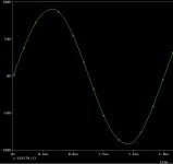
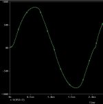
The circuit below gives 200V Pk-Pk into a 1K load from DC to 500KHz with low distortion. Idling current is 10mA and frequency response is -3dB at about 1MHz.
If two are bridged to get 400V Pk-Pk across the load, they can both be driven from a PNP long tailed pair biased at earth potential.
To get higher speed, replace Q2 and Q3 with 2SC3503 and increase the idling current in the first stage. Replacing R1 with a current source would improve performance too.
Attachments
- Status
- This old topic is closed. If you want to reopen this topic, contact a moderator using the "Report Post" button.
- Home
- Amplifiers
- Solid State
- Wide bandwidth class AB with 10mA quiescent?