So I should have instead of two twisted pairs(see pic in post 102), done a twisted triplet with the two caps sharing one ground. Damn, I almost did that too but decided it was safer to separate the 2 into flow and return.
I understand that the power rails should be close coupled on the PCB but I am still in the strip board stage. I am planning on getting custom PCBs made in the future so keep the tips coming as to the proper way.
The main thing that I get hung up on is the fact that the longest run of wire always seems to be from the PSU to the PCB with the amps on it. Everything I read stresses the importance of the HF 100nF bypass caps having as short of leads as possible but that seems impossible if the PSU is so far away. I have just been using one 100nF ceramic per package and tying both power pins to it because of this. Is this not effective for the HF?
I have 7 dual channel op amps on my board at the moment so needless to say there are quite a few signal grounds to deal with. Andrew, I am starting to understand what you are saying about the importance of a local decoupling ground (I assume this should be on the preamp PCB). Should there be a local signal ground kept separate from the decoupling ground to avoid noise from changing currents on the PCB as well? And then attach that to "Somewhere along the d.) connection you tie into the Main Audio Ground." -this point?
Speaking of inductance and impedance, is there a certain gauge of wire that is best to use for the wiring of a preamp?
Mark, I am unclear on what the grounding arrangement you feel is best, do you mind explaining how you would wire the ground from the PSU to the PCB and where the incoming signal ground would connect?
Speaking of inductance and impedance, is there a certain gauge of wire that is best to use for the wiring of a preamp?
At 20kHz, the skin depth in copper is about 0.45mm. If we choose a wire radius equal to one skin depth, the diameter is 0.9mm, or a wire gauge of #19.
This would be about the largest diameter of wire to use if you want to keep the AC resistance of the wire from varying too much with frequency through
the audio band. I normally use #20 wire in preamps.
They connect to the devices pins and the local ground, you don't take their GND pins all the way back to the main PSU.The main thing that I get hung up on is the fact that the longest run of wire always seems to be from the PSU to the PCB with the amps on it. Everything I read stresses the importance of the HF 100nF bypass caps having as short of leads as possible but that seems impossible if the PSU is so far away. I have just been using one 100nF ceramic per package and tying both power pins to it because of this. Is this not effective for the HF?
There is a wealth of information regarding skin effect at Audio frequencies.....no effect.
The grounding and decoupling discussed previously only differs by 10 mm of trace, which is about 10 nH of inductance and is more relative to chipamps.
Now back to the Shredhead preamp.
Lets start with the PSU. I would build two regulated PSU's, One with + and GND, the other with - and GND. (They are really identical except for the markings at the connectors.)
On the preamp board, place two small caps (100-500 uF) at the power rails.
Whatever the datasheet recommends for local decoupling. If it's rail to rail, run two traces to all of the opamps and place a small cap (0.1 uF) at the opamps power pins. If it's rail to ground, I would add a power ground plane under the two traces going to the opamps and place one cap (0.1 uF) per rail at the opamps pins.
Then the audio layout. I would run the signal and its GND together through the board. Analyse the schematic to see where the loops are. Make it a priority to keep the loops small (and short). Where will inductance cause problems? Which component can't be placed together? It can be found in the datasheets.
Connect the audio GNDs to the power GND, near the outputs. For multiple channels use resistors to reduce ground loops where necessary and where it will not send the audio GND signal down an alternate route.
As you have already demonstrated, it is a very good thing not to connect the audio GNDs to the chassis. Insulate inputs and outputs from the chassis.
Connect the preamp to the PSU with four leads +, GND, -, GND. Connect a third power GND lead from the preamp to the chassis. For this connection you can use a ground loop breaker.
Finally connect the mains earth/GND to the chassis.
Now there are some things you could do differently.
Place the voltage regulators on the preamp board. You will need to do that if the devices don't use the same supply voltages.
You could build a different type of PSU, one with a single GND and a centre tap transformer, but that would change the ground layout.
Last edited:
I missed that point.I am not connecting the HF caps to the PSU, but directly to the MF caps of each rail.
And it was me that pointed out the MF to HF current flow.
AndrewT and I only disagree on how the ground layout should be done. HF to HF or HF to MF as a priority.
That's why I kept asking for explanation.
I connect HF to HF and MF to MF and then connect these two common points together with a very short link. This makes the inner loops very small, and the MF loops slightly bigger.
This matches up with Marce's keep the local loops small and progressively move out the the slightly bigger loops of the MF and the much bigger loops of the main smoothing.
There is no current flow HF to HF or MF to MF. You have the lowest inductance between caps with no current flow and a higher inductance between caps with the highest current flow.
In layout terms connect one HF and one MF cap with short wide trace to ground or even better use a single ground plane.
If you know these current exist, you can try to keep them out of the input and output GNDs.
In layout terms connect one HF and one MF cap with short wide trace to ground or even better use a single ground plane.
If you know these current exist, you can try to keep them out of the input and output GNDs.
for an AC waveform of the shortest pulse time (highest HF) first one HF cap supplies the amplifier current and returns to the decoupling node. Then the other HF cap supplies the other half waveform and returns that to the same node when HF is connected to HF.
The other loops become insignificant during the period of fast current changes.
After that, the MF recharge the HF and also supply longer duration pulses.
I think of it as what decoupling ground arrangement works for the very highest frequencies first. To me that is HF to HF.
The recharging comes later and uses the longer loops.
The recharge does not wait until the half wave cycle has ended.
It looks more like this:
Take an AC waveform and divide it into four quarters. The first quarter the current flows from the positive HF cap and PSU + to the chip. The second quarter, the PSU is still supplying current to the chip but the positive HF cap current has reversed. The first two quarters there is almost no current from the negative rail. The third quarter. It is now the negative rail turn. Negative HF cap and PSU - supply current to the chip. Forth quarter, reverse of the current through the negative HF cap. PSU - still supplying current to the chip.
Most of the HF cap recharge current is received during it own rail cycle.
There can be an overlap when one HF cap is recharging and the other is supplying, the resulting current flows down the short trace to GND. The only way to get rail to rail current is if both caps are acting in the same cycle, supplying or charging.
Last edited:
I sketched out the HF to HF (very short loops) with the longer loops for MF to MF and added in the Zobel.
Compared this to what I think you are describing for HF to MF and HF to MF then both to a common ground and added the same Zobel.
In the second sketch it is very clear that the loops for the HF must be longer than in the HF to HF case.
I still think the priority should be to minimise the loop length of the two HF routes.
You posted a sim plot. Could you post the diagram that you used for this and explain what the various traces show.
I would like to compare the HF to HF version to the HF to MF version to see if the sim can differentiate between them.
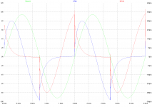
For HF to HF current, there must be a positive and a negative current at the same time. (The blue above 0 and the red below 0.) as you can see this never happens.
You can also see a 90 degree phase shift of the total HF current relative to the output signal.
You can also see a 90 degree phase shift of the total HF current relative to the output signal.
Attachments
Last edited:
Who claimed that current can pass simultaneously through the decoupling capacitors. I certainly didn't.
Go back to the rather nice analogy I copied:
Imagine each HF decoupling capacitor as a battery. Each battery can supply current for a short time before becoming significantly depleted. During that short period this is the ONLY power supply for the amplifier and as the ONLY source of power all the curent that leaves the source must return to the source. i.e. ONE decoupling capacitor forms it's sole current route into and out of the amplifier.
Let's say the current supply lasts 1us and then requires recharging from the MF decoupling which too becomes significantly depleted after 100us.
On a positive pulse that lasts from start to end for 1us (500ns rise time and 500ns fall time), the battery supplies the current and it's voltage falls.
Then the pulse is negative. The other battery supplies current for this -ve pulse and it too depletes a bit. During this time the -ve battery has partially recharged from the MF.
The there is a short period of no pulses, the +ve battery continues and the -ve battery starts recharging.
After a delay of say 50us there is a further -ve pulse followed by a +ve pulse. The depleting and recharging follows the same pattern as before.
I note in your sim sch that HF decoupling has been omitted.
100nF is commonly used.
1mm leads are possible.
That results in 1nH of inductance on both sides of the HF capacitor
MF decoupling typically has leads of the order of 10mm to 30mm length. That would result in a typical inductance on BOTH sides of the MF decoupling of ~20nH.
Could you post the asc so that I can insert these?
Last edited:
AndrewT, I think the analogy you posted is very helpful.
1. Which is the better configuration for the batteries? Y or V.
2. Where/how would you connect the battery chargers for each option?
1. Which is the better configuration for the batteries? Y or V.
2. Where/how would you connect the battery chargers for each option?
Thanks for the breakdown of the wiring Mark. I appreciate you guys getting into the "battery recharging", it has given me new things to think about.
Figuring on a local decoupling ground plane, would it make sense to also have a separate local ground plane for the audio signal that has it's own dedicated feed back to the PSU? I know this would create a pretty large loop but if you kept both ground feeds tied close together, do you think it would be beneficial for keeping pulse noise out of the signal or problematic?
Figuring on a local decoupling ground plane, would it make sense to also have a separate local ground plane for the audio signal that has it's own dedicated feed back to the PSU? I know this would create a pretty large loop but if you kept both ground feeds tied close together, do you think it would be beneficial for keeping pulse noise out of the signal or problematic?
Last edited:
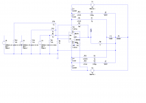
I have been working with Mark's asc for the past few hours trying to understand how the decoupling behaves with very fast signals.
I did see a strong second harmonic on the HF cap current. I suspect this is ringing due to insufficient damping with the very low resistances in there. I increased them by a few decades to reduce the 2nd harmonic.
I will post my modified version of the HF to HF version as soon as I discover how to get it into an attachment.
How do I replace the sinewave test signals with fast pulses of one or two pulses duration?
I would like to see the sim modeling for that?
I have converted the sim to HF to MF and will start analysing that to see if it gives different results.
Shred,
multi-layer PCBs do not use two layers.
Generally they use at least 4layers and preferably 6 or more.
As I understand it after just one reading they typically have:
power ground, +power, -power, ground plane, signal traces, signal ground plane
The signal traces are buried between two ground planes.
The power traces are buried between two ground planes.
The power and signals are separated by a ground plane.
H.Ott discusses this in detail, it's not until he gets to about 8layers that the disadvantages of each of the fewer layers PCBs drops down to none.
But since I will never try to design a multi-plane PCB, I have not tried to memorise any of his design rules.
I know my limitations and ground planes is beyond where I need to go for audio frequencies.
I have disconnected the 500Hz signal and connected the 20kHz signal
Changed that to 500kHz or 800kHz or 1Mhz
added in parasitic inductances around every capacitor.
added main smoothing capacitors.
Changed the 3886 to lt1037 since I knew that was fairly fast and was not unity gain stable (similar to 3886 but faster)
added a Zobel and increased the speaker load to 1k.
added L25, 26 & 27 to simulate internal lead in wiring inside the chipamp package.
After seeing the strong 2nd harmonic on the HF decoupling cap I have increased substantially the parasitic resistances.
I did a lot of zooming in to see details of the voltage and current waveforms.
edit
That opened correctly !
Note
I have relabeled many of the resistors/inductors to indicate their function when looking at the plots after "run".
I+hf = the +ve polarity current through the resistor leading from the HF decoupling capacitor. It reverses into a -ve current when recharging.
I+opamp = the +ve polarity current into the opamp +ve lead.
I+supply = current from the voltage source that simulates the rectified AC from the transformer.
I-mf = the -ve polarity current from the MF decoupling.
One important lesson.
Even though the voltage source is the main current source for the amplifier, I can see the VERY small variation in current from here. It operates as almost a perfect DC constant current supply.
The Main Smoothing capacitors have small current variation that is in phase with the MF decoupling cap current, but again the variation is very small. There is not much AC demand on the Main Smoothing.
I.e. the PSU is a DC supply with very little transient requirement when the decoupling can cope with the demand from very fast transients.
If one puts back in the 500Hz signal and looks again at the Main Smoothing current, one sees the "slow" demand being met by the "slow" capacitors. The decoupling exhausts itself too quickly to have any significant effect on maintaining near constant voltage on the supply pins when the currents CHANGE SLOWLY.
Attachments
Last edited:
AndrewT, Did you have fun?
The parts used are real parts and not tweaked to remove ringing. I want to simulate an actual PSU with real AC current demand to see what is happening. The three AC supplies are an attempt at simulating an audio signal.
I had previously used AC supplies and diodes as a supply but they prevented AC analysis (loop gain e.t.c).
I don't think you can call it "Exhausts". it is a small local lowering of the voltage at the HF capacitors which later forces the other caps to take over. This also explains the recharge.
The zobel is causing a much lower impedance at HF. This increases the HF current demand compared to the LF demand.
Thanks for the breakdown of the wiring Mark. I appreciate you guys getting into the "battery recharging", it has given me new things to think about.
Figuring on a local decoupling ground plane, would it make sense to also have a separate local ground plane for the audio signal that has it's own dedicated feed back to the PSU? I know this would create a pretty large loop but if you kept both ground feeds tied close together, do you think it would be beneficial for keeping pulse noise out of the signal or problematic?
If you run the audio ground/return traces as if they are audio supplies it will improve channel separation and you can also build ground loop breakers into the design. (low noice)
I have seen a multi channel layout where all the input grounds are connected together, all the opamp grounds are connected together, al the feedback grounds are connected together and all the output grounds are connected together. The four grounds are connected to the power ground. The designer had not considered the audio signal flow at all.
I know my limitations and ground planes is beyond where I need to go for audio frequencies.
I am considering a 2 sided board with just 1 ground plane. Any more than that seems to drive the cost up too much. I was thinking of splitting the 1 ground plane in half. One side for local decoupling and the other for signal grounds, trying to keep the routes as short as I can get them.
Are you saying that you use 1 sided primarily? I guess you probably work on power amp stuff more than pre amps. I hope to get into more of the amp side of things next year. I've only done some chip amps so far which doesn't really teach you anything about the fundamentals. Do you have any suggestions on a book to help with an understanding of discrete power amps?
I have seen a multi channel layout where all the input grounds are connected together, all the opamp grounds are connected together, al the feedback grounds are connected together and all the output grounds are connected together. The four grounds are connected to the power ground. The designer had not considered the audio signal flow at all.
Multi channel seems to be the most challenging when it comes to low noise. I've run across some name brand 5.1 stuff even that has crap S/N figures and it isn't cheap stuff. I find it hard to explain this. Are the principals of signal flow not common knowledge to most designers?
- Status
- Not open for further replies.
- Home
- Source & Line
- Analog Line Level
- Which one of these wiring schemes will have lower noise?