I don't know what you have described.The op amps power pin's bypass caps are traveling back to the star ground near the PSU and away from the signal ground point.
Can you post a drawing and/or a pic?
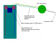
I used a kind of power buss to jump off of to feed the op amps. This shows how I wired the electrolytic bypass caps for the power coming into the board. The ground connection to each capacitor goes back to the higher current PSU ground point instead of the signal ground on the PCB. I didn't show the ceramics on the op amps because this program I use to draw things makes me want to kick a hole in the wall.
Attachments
I don't think that is an effective way to couple the local decoupling.
The Ceramics are the High Frequency (HF) decoupling they supply current for typically 1us transient demand. They must be connected to the opamp supply pins as close to the package as physically possible.
They then need to be connected together to create a local HF Decoupling Ground. These last two connections must be just as short as the pin connections. It's the LOOP length and LOOP AREA that must be kept very small.
The small electrolytics are the Medium Frequency (MF) decoupling. These should be fairly close to the package pins but because they supply the MF they will tolerate longer Loops than the HF. BUT !!!!! the cap to cap length MUST be just as short as the power side connections. NOT back to a remote star ground.
Connect the two electrolytics together to create an MF local decoupling ground.
Connect the MF Decoupling Ground to the HF Decoupling Ground using a short direct wire/trace. This wire trace is the PCB Power Ground. Any Fast (HF) current returning from the load or from the Zobel should be brought back to this low impedance trace/wire.
I described this to Tom asking for his comments after he said I was wrong. Despite the invite to discuss this wiring philosophy he has remained silent.
So for the time being, or until someone convinces me that this low impedance decoupling grounding point is flawed, I recommend it.
Consider the Zobel. It is a load on the output and any current flowing through it must return to the Power Ground. Which Power Ground?
The Zobel ONLY passes HF signals, the ~100nF ensures this is so. It does not pass Audio Signals.
HF signals must return to a low impedance ground. They will not tolerate a long open loop (high impedance due to inductance). I see the only place to return the Zobel currents is to the low impedance local Decoupling Ground. The short wire between the HF and MF decoupling grounds is in my view the ideal location. The returning current arrives at the short HF to MF wire/trace and has a choice of routes, either the to HF side, or to the MF side. The two routes are effectively in parallel.
As I see it, the chipamp/opamp/poweramp must have a local decoupling ground.
Here we have the
a.) the HF decoupling ground
b.) the MF decoupling ground
c.) the Zobel Return
d.) the connection to take this point to the Power Supply.
Somewhere along the d.) connection you tie into the Main Audio Ground.
This Main Audio Ground is also the reference point where any other parts of the circuit make their REFERENCE connection for correct operation. eg. the Signal Return/Ground ties in here.
Last edited:
Andrew T, what you have not considered is the current flow from the MF caps to the HF caps and the current flow from the PSU to the MF caps.
There are more loops than you may expect.
There are more loops than you may expect.
The way I see it is that after a capacitor supplies current it will need to be recharged from the upstream capacitors.
We have two capacitors, HF and MF. If the opamp demands HF current it will mostly be supplied by the HF capacitor. As the HF current demand ends there will be a voltage imbalance between the two capacitors, a current will flow from the upstream caps into the HF cap. The capacitor with the next lowest inductance will supply most of this current.
Now you can apply this to the ground configuration you want to use.
Last edited:
Yes, I agree.
The MF decoupling recharges the HF decoupling as fast as it's able.
The remote main smoothing capacitance then has the job to recharge the MF decoupling.
The lowest impedance is right at the decoupling grounds. Any further away and the impedance becomes too high for fast current changes.
Remotely located capacitance can only supply slowly changing current. All the fast changes in demand are met by the local decoupling and returned to the low impedance node between the local decoupling capacitors.
The slowly changing demands are met by ALL the capacitors, even those at the far ends of long cables.
But, to minimise interference of the changing currents, the flow and return routes must be close coupled.
That's the reason for the twisted pairs in ALL cable pairs. And the twisted triplet where we have a dual polarity supply.
If you use a HF ground and a MF ground you have increased the inductance of the ground route between the HF and MF capacitors. If the current flows from the MF to the HF caps. The same current must flow from HF to MF though the ground.
Then there is a second problem. The current flow though HF and MF decoupling grounds are supplied from both the positive and the negative rails.
Apply the twisted pairs theory to the HF and MF caps. The supplies and grounds need to run parallel.
Then there is a second problem. The current flow though HF and MF decoupling grounds are supplied from both the positive and the negative rails.
Apply the twisted pairs theory to the HF and MF caps. The supplies and grounds need to run parallel.
Last edited:
You are misunderstanding the linking of the capacitors.
The HF decoupling ground must be located in the shortest total route.
This takes some space.
The MF decoupling route then becomes second priority and although a short total route is adopted must necessarily be longer than the HF. It's the combination of longer route and electrolytic capacitors that make this the MF decoupling.
Now join the two decoupling grounds together by the shortest trace/wire. the capacitor layout will determine just how short this MF route will be: maybe 10mm of trace between the two electolytics, hopefully less than 20mm of trace.
There will be some finite length/distance between the HF ground an this MF ground.
Choose a point somewhere along this trace/wire.
That point becomes the decoupling ground that connects with the rest of the world/PCB.
Any fast changing return currents arriving at that point have a choice of routes. Either through the HF decoupling or through the MF decoupling.
Since there is a choice of routes they are in parallel.
Two impedances, even when one is significantly higher than the other, when in parallel will result in a lower effective impedance. The returning currents will proportion themselves to return to their Source Capacitor.
Once the Main smoothing capacitors are added to the power grounding, we have introduced a third parallel route for returning currents.
I keep reminding Members that the amp PCB must keep the supply wires/traces close coupled.
I see many PCB layouts that separate the supplies and place them on opposite sides of the PCB. This is the opposite of close coupled. But they won't listen.
The HF decoupling ground must be located in the shortest total route.
This takes some space.
The MF decoupling route then becomes second priority and although a short total route is adopted must necessarily be longer than the HF. It's the combination of longer route and electrolytic capacitors that make this the MF decoupling.
Now join the two decoupling grounds together by the shortest trace/wire. the capacitor layout will determine just how short this MF route will be: maybe 10mm of trace between the two electolytics, hopefully less than 20mm of trace.
There will be some finite length/distance between the HF ground an this MF ground.
Choose a point somewhere along this trace/wire.
That point becomes the decoupling ground that connects with the rest of the world/PCB.
Any fast changing return currents arriving at that point have a choice of routes. Either through the HF decoupling or through the MF decoupling.
Since there is a choice of routes they are in parallel.
Two impedances, even when one is significantly higher than the other, when in parallel will result in a lower effective impedance. The returning currents will proportion themselves to return to their Source Capacitor.
Once the Main smoothing capacitors are added to the power grounding, we have introduced a third parallel route for returning currents.
I have been making this point for years. Cherry talks about it around 1996 (his article, or a link to it, has been posted on this Forum). I keep reminding Members to bring the supplies to the amplifier as a twisted triplet.The current flow though HF and MF decoupling grounds are supplied from both the positive and the negative rails.
I keep reminding Members that the amp PCB must keep the supply wires/traces close coupled.
I see many PCB layouts that separate the supplies and place them on opposite sides of the PCB. This is the opposite of close coupled. But they won't listen.
Last edited:
During the recharge of the HF caps the HF and MF caps form a current loop. The sum of the inductance of the loop is what is important. The inductance of one HF cap, one MF cap and the two traces connecting them.
Here you can see the positive opamp, PSU, MF and HF currents.
Here you can see the positive opamp, PSU, MF and HF currents.
Attachments

Last edited:
Yes, Tell me what the colours indicate?
What is the point you are making?
you are back to the original comment
The two pairs of capacitors already have the shortest route lengths and PCBs only have multi-layering to help with the non twisted technique of lowering impedance.
One cannot twist the traces and one cannot bring the routes any closer together.
What this does bring out is that small components can be much closer together and that this has a direct effect on impedance.
What is the point you are making?
you are back to the original comment
I can't see where my logic is flawed nor where your question is directing my thoughts/tests/simulations/modeling.what you have not considered is the current flow from the MF caps to the HF caps and the current flow from the PSU to the MF caps.
There are more loops than you may expect.
The two pairs of capacitors already have the shortest route lengths and PCBs only have multi-layering to help with the non twisted technique of lowering impedance.
One cannot twist the traces and one cannot bring the routes any closer together.
What this does bring out is that small components can be much closer together and that this has a direct effect on impedance.
Last edited:
I don't see the advantage of connecting the two HF caps together forming a separate ground.
It is +CLC- with AC current flowing +CL GND and GND LC-, there is almost no current flowing +CC-
I(R3) is the current entering the chip from the positive rail.
I(L2) is the current from the PSU.
I(R1) is the current though MF cap to the positive rial.
I(R2) is the current though HF cap to the positive rail, relatively small.
Last edited:
The two sets of caps need to be connected to the PSU Zero Volts.
It seems better to connect them locally and run one trace/wire to the PSU.
That local connection becomes the lowest impedance for the power currents on the PCB
It seems better to connect them locally and run one trace/wire to the PSU.
That local connection becomes the lowest impedance for the power currents on the PCB
Originally Posted by AndrewT
Post # 103
d.) the connection to take this point to the Power Supply.
Somewhere along the d.) connection you tie into the Main Audio Ground.
This Main Audio Ground is also the reference point where any other parts of the circuit make their REFERENCE connection for correct operation. eg. the Signal Return/Ground ties in here.
Post # 113
The two sets of caps need to be connected to the PSU Zero Volts.
It seems better to connect them locally and run one trace/wire to the PSU.
That local connection becomes the lowest impedance for the power currents on the PCB
There seems to be a contradiction between your two posts, which i've Bolded ?
The two sets of caps need to be connected to the PSU Zero Volts.
It seems better to connect them locally and run one trace/wire to the PSU.
That local connection becomes the lowest impedance for the power currents on the PCB
It is probably a twisted way at approaching the problem but I want to create a zero volt point at the amp and not at the PSU.
everything cannot be located at or in the "point" between the two HF decoupling caps.
Some compromise has to be made.
The fastest currents (what I call HF) go straight into the HF decoupling ground.
The medium speed changing currents (MF) go to the MF decoupling ground and thence to the HF decoupling ground by the shortest route available.
That route for the connection from HF to MF decoupling must have a finite length.
Some where along that length we fix a connection for the slowest (mostly audio signals) changing currents.
This midway connection sees both the HF and HF decoupling grounds and at a somewhat greater distance we have the main PSU smoothing.
We could have some intermediate decoupling at the input to the PCB, but relative the the tiny lengths involved in laying out the HF & MF, this is still a big distance away.
ZeroD has picked up an apparent contradiction and you are introducing the same thing when you say
We have a remote PSU and in there we have the PSU Zero Volts. This is a DC Zero Volts, due to impedance of the long inductive wiring, it must have a varying AC voltage around the DC value.
Close to the amplifier, we create a Main Audio Ground (MAG) (in a Monoblock this can be on the single channel amplifier PCB). I have suggested that the Main Audio Ground be near the centroid of
e.) the input socket,
f.) the output socket,
g.) the amplifier input terminal,
h.) the amplifier output terminal.
But there is a connection between the decoupling ground and the main audio ground and the PSU Zero Volts.
I consider the PSU Zero Volts as the least important and as a result have not included it in the list e to h.
There is a lot of leaway here and the fact that many Builders do not adhere to this and still get good performance confirms that the MAG can be located away from some, or many, of those location conditions.
Ultimately any current that comes OUT of the PSU, MUST return to the PSU.
It MUST be included in the decoupling route, but due to space considerations cannot be in the "point".
The MAG seems of much higher priority, simply due to the need to minimise the impedance in the connection from decoupling ground to the main reference point that other parts of the amplifier need to use.
The MAG should be relatively close to the decoupling ground.
Choose to put it on the PCB if a Monoblock, or near the PCB if a multi-channel amplifier. I have even suggested locating the MAG on the Speaker Return Terminal.
This is where the locations of e to f come back in. These parts of the amplifier all operate at roughly the same voltage as the MAG. Any voltage difference between any of those points is an error. Minimise the voltage errors by minimising the impedance.
Closeness helps achieve that. Separation of the different currents helps achieve that (is this where star grounding originates?).
But physical coincidence at an infinitely small "point" is not achievable, it can never be a reasonable target.
Even multi-layer PCBs cannot get there, one finds that layer to layer distances and via locations and component orientations all have an effect on impedance. Impedance can never be Zero.
Some compromise is required. The biggest voltage errors result from the fastest currents and/or the largest currents.
Both benefit from closeness of the components/assemblies.
Some compromise has to be made.
The fastest currents (what I call HF) go straight into the HF decoupling ground.
The medium speed changing currents (MF) go to the MF decoupling ground and thence to the HF decoupling ground by the shortest route available.
That route for the connection from HF to MF decoupling must have a finite length.
Some where along that length we fix a connection for the slowest (mostly audio signals) changing currents.
This midway connection sees both the HF and HF decoupling grounds and at a somewhat greater distance we have the main PSU smoothing.
We could have some intermediate decoupling at the input to the PCB, but relative the the tiny lengths involved in laying out the HF & MF, this is still a big distance away.
ZeroD has picked up an apparent contradiction and you are introducing the same thing when you say
I refer back to my postI want to create a zero volt point at the amp and not at the PSU.
I have added in a missing comma, that maybe helps with interpretation.the chipamp/opamp/poweramp must have a local decoupling ground.
Here we have the
a.) the HF decoupling ground
b.) the MF decoupling ground
c.) the Zobel Return
d.) the connection to take this point to the Power Supply.
Somewhere along the d.) connection, you tie into the Main Audio Ground .
We have a remote PSU and in there we have the PSU Zero Volts. This is a DC Zero Volts, due to impedance of the long inductive wiring, it must have a varying AC voltage around the DC value.
Close to the amplifier, we create a Main Audio Ground (MAG) (in a Monoblock this can be on the single channel amplifier PCB). I have suggested that the Main Audio Ground be near the centroid of
e.) the input socket,
f.) the output socket,
g.) the amplifier input terminal,
h.) the amplifier output terminal.
But there is a connection between the decoupling ground and the main audio ground and the PSU Zero Volts.
I consider the PSU Zero Volts as the least important and as a result have not included it in the list e to h.
There is a lot of leaway here and the fact that many Builders do not adhere to this and still get good performance confirms that the MAG can be located away from some, or many, of those location conditions.
Ultimately any current that comes OUT of the PSU, MUST return to the PSU.
It MUST be included in the decoupling route, but due to space considerations cannot be in the "point".
The MAG seems of much higher priority, simply due to the need to minimise the impedance in the connection from decoupling ground to the main reference point that other parts of the amplifier need to use.
The MAG should be relatively close to the decoupling ground.
Choose to put it on the PCB if a Monoblock, or near the PCB if a multi-channel amplifier. I have even suggested locating the MAG on the Speaker Return Terminal.
This is where the locations of e to f come back in. These parts of the amplifier all operate at roughly the same voltage as the MAG. Any voltage difference between any of those points is an error. Minimise the voltage errors by minimising the impedance.
Closeness helps achieve that. Separation of the different currents helps achieve that (is this where star grounding originates?).
But physical coincidence at an infinitely small "point" is not achievable, it can never be a reasonable target.
Even multi-layer PCBs cannot get there, one finds that layer to layer distances and via locations and component orientations all have an effect on impedance. Impedance can never be Zero.
Some compromise is required. The biggest voltage errors result from the fastest currents and/or the largest currents.
Both benefit from closeness of the components/assemblies.
Last edited:
This does seem to be getting rather complex to my poor little brain.
on all the analogue designs I seem to work on (Audio is analogue) do not split grounds into HF MF decoupling grounds and generally keep things simpler, much simpler. I also think that some are looking at loops that are too large going all the way back to the main PSU, the whole point of decoupling is to create smaller loop areas where the caps supply the instantaneous power....Keep things simple is my motto. But then I would not do low level analogue without a ground plane....
on all the analogue designs I seem to work on (Audio is analogue) do not split grounds into HF MF decoupling grounds and generally keep things simpler, much simpler. I also think that some are looking at loops that are too large going all the way back to the main PSU, the whole point of decoupling is to create smaller loop areas where the caps supply the instantaneous power....Keep things simple is my motto. But then I would not do low level analogue without a ground plane....
I also think that some are looking at loops that are too large going all the way back to the main PSU,
I don't agree with this. In simulations I have increased the inductance at the PSU to see the amp's HF caps oscillate.
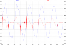
Here a plot of the output voltage and the current of the positive HF cap with a slightly high inductance in the supply and ground rails from the PSU.
Attachments
Last edited:
The small decoupling caps next to the ICs form a small loop for the instantaneous power requirements, then as Andrew points out there is another loop where any reservoir caps (MF decoupling) supply the HF (local decoupling) caps, and so on back to the main power supply....having the local decouplers (HF) caps ground connection go all the way back to the main PSU minimises their effectiveness as the added inductance (the killer for local caps). What I am saying is look at the local small loops, staring everything back to some distant point just adds inductance.
As I said all low level (and higher current) analogue I see uses a ground plane (high power currents get there own, and often there is a separate input ground to form an EMC moat connected at a star point) with generally a power connector for external power of a PSU on board.
So we concentrate on keeping the various inter circuitry loops as small and neat as possible, using placement and routing to minimise any interference between areas of circuitry........
I am not connecting the HF caps to the PSU, but directly to the MF caps of each rail.
And it was me that pointed out the MF to HF current flow.
AndrewT and I only disagree on how the ground layout should be done. HF to HF or HF to MF as a priority.
And it was me that pointed out the MF to HF current flow.
AndrewT and I only disagree on how the ground layout should be done. HF to HF or HF to MF as a priority.
- Status
- Not open for further replies.
- Home
- Source & Line
- Analog Line Level
- Which one of these wiring schemes will have lower noise?