Hi,
some say that a mirror on the LTP does not sound as nice as a resistor feed. You tell us after testing.
If you go dual complementary LTP into complementary VAS then you cannot use mirrors on the LTPs, you need resistor feeds to stabilise the VAS idle current.
Read Leach on GBW product & particularly what happens if you increase the gain too far & try to slug it down again with an excess of NFB. A number of other authors state similar without all the theory to back it up. In fact read ALL of Leach! & then D. Self followed by JLH. Gives a good balance of different styles and will teach you a lot quickly. But you'll still come back to DIYaudio to fill in the gaps and hear the pragmatic approach.
I recommend emitter resistors (everywhere?) on all the important transistors. At least leave space on your PCB for them & then optionally link them out for testing/evaluation.
Of course you can't. Thanks Andrew. Stick with the resistors and add a cascode if you can. You can also cascode the Vas to reduce distortion. And don't forget to degenerate those diff'l pairs to reduce the need for comp. Use feedback lead comp.
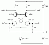
Ag, what is your take on complementary FET plus bootstrapped cascode front end (keeps Vds on FETs constant to reduce impact of nonlinear Cds).
The problem I see there is you are bootstrapping the cascode off of the feedback (or dedicated output divider, not much of a difference really in this case) which means that you probably get sharply rising THD at high freq once the bootstrap starts lagging, and probably worse further up the frequency band as previously bootstrapped Cds starts doing it's Miller thing..
The problem I see there is you are bootstrapping the cascode off of the feedback (or dedicated output divider, not much of a difference really in this case) which means that you probably get sharply rising THD at high freq once the bootstrap starts lagging, and probably worse further up the frequency band as previously bootstrapped Cds starts doing it's Miller thing..
schema
Hi
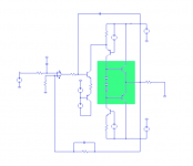
I try to understand what kind of circuit is under discussion. A green box in attached file just indicate a place for output stage, not a real OS.
But other part may be real. OpAmp like OPA603.
Is this circuit fit to the block diagram from p.60?
What kind of real circuit more or less fit to described design?
Hi
I try to understand what kind of circuit is under discussion. A green box in attached file just indicate a place for output stage, not a real OS.
But other part may be real. OpAmp like OPA603.
Is this circuit fit to the block diagram from p.60?
What kind of real circuit more or less fit to described design?
Attachments
AndrewT said:Hi Ilimzn,
what is a bootstrapped cascode?
Are you able to post a sketch?
I am attaching a sketch - just for reference, the part values are not representative. The voltage source fixes the Ugs of the JFETs, if the FET was an ideal follower, the voltage swing seen by Cds and Cgs would be zero.
Since the real version of this circuit would require a relatively low impedance node at JFET source potential, it is taken from the feedback divider or from a dedicated divider with the same resistor ratio. It is also possible to connect it as it is on the sketch - all approaches have virtues and flaws...
Attachments
Ilimzn,
That's a very interesting JFET connection.
I guess a constant voltage across the JFET will improve its linearity as a pure transconductance amp (gate voltage in, current variation out).
However, the curves lead me to think that any deviation in Idss, and I assume we are operating these JFETs with zero gate bias, should preferably be accompanied by a tiny variation in voltage across the device. That is, increase JFET current, and decrease voltage across it as a form of negative feedback, fully linearizing the JFET.
And is constant voltage operation of the JFET by using the cascode really the best way to go, since gain is simply gm x RL?
What do you think?
Cheers,
Hugh
AKSA said:Ilimzn,
That's a very interesting JFET connection.
I guess a constant voltage across the JFET will improve its linearity as a pure transconductance amp (gate voltage in, current variation out).
However, the curves lead me to think that any deviation in Idss, and I assume we are operating these JFETs with zero gate bias, should preferably be accompanied by a tiny variation in voltage across the device. That is, increase JFET current, and decrease voltage across it as a form of negative feedback, fully linearizing the JFET.
I assume you meant Id not Idss (Idss = Id @ Vgs=0).
Please note that the circuit above just shows the principle, the main feature being a voltage source between JFET Ss and cascode Bs (BTW this circuit can have many variations, not just a LTP). In a real implementation, as I stated, the Bs of the cascode can be derived in many different ways, for instance a voltage divider, or bootstrapping 'degeneration; can be introduced by adding suitable value resistors in the Ds of the JFETs.
Your suggestion certainly deserves serious consideration, and do plan to investigate this when time alowes. The tradeoff is balancing the nonlinearity of the JFET transfer characteristic and the nonlinearity of Cgd with voltage. This will vary with JFET chosen as well as DC operating points. A simulator with reasonable JFET models should be a good tool to test this and at some point in time, I probably will 😉
The good thing with FETs is that units with fairly large Idss are common, which means a large tail current is used WRT typical BJT LTP implementations. This makes it easy to use a regular voltage divider from +Vcc to the common source point of the JFETs, since typical base currents for the cascode BJTs will be small compared to the tail current (bypass caps need to be used as appropriate, of course, to set proper AC returns and/or ratios vs DC operating point). MOSFETs can also be used with this topology with similar benefits.
This above approach eliminates one problem from my original question: the bootstraping (which is a form of positive feedback) loop is short and mostly confined to this stage, and limits the bootstraping to any value from 0 (Bs of cascode at AC ground) to ~~Vin (Bs of cascode and Ss of JFETs AC connected like in sketch above), so no problem with stability. Deriving the bootstrap in different ways gives more flexibility but also a danger of oscilation.
And is constant voltage operation of the JFET by using the cascode really the best way to go, since gain is simply gm x RL?
Well, since the cascode BJTs have Av~~1 you are limited to gm*Rl anyway, that is as long as you use a resistive load - and as long as you do you cannot escape relatively low JFET and MOSFET gm. Keep in mind that resistors in the sketch were just shown to make the circuit complete, they are not representative at all.
Decent voltage gain from this circuit requires an active load (eg. current mirror), or you use current drive for the next stage. Using this circuit as the front end of an amp feeding a BJT VAS would probably work just fine with resistors as shown (tail currents for JFET inputs tend to be quite high, so plenty of drive current is available). If you wanted to drive a MOSFET, voltage swings need to be considered, so different arrangements might be used.
Upupa Epops said:Hi Hugh, nothing new 😎 . Is thruth, that this combination give much more better sound results than the same with bipolars.
There is one small but crucial difference between my sketch and the schematic you posted - in your schematic the JFETs are connected to a regular cascode without bootstrapping, which means Vds is not constant, but has an AC component roughly equal to the common mode voltage of the LTP (in actuality somewhat smaller as JFETs are not perfect followers due to finite gm), that in turn, is roughly equal to the input signal.
That being said, the schematic I posted indeed isn't anything new - I am not taking any credit for it, though I have not seen it widely used.
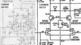
Hi,
did Luxman & Sansui have the same designer at some time?
What effect does the bootstrapping have either on measured output or on the sound quality?
Are there any disadvantages?
did Luxman & Sansui have the same designer at some time?
What effect does the bootstrapping have either on measured output or on the sound quality?
Are there any disadvantages?
amplifierguru said:
No cascode in diff stage, yes?
No
Keep it simple and let NFB to do the job?
absolutely
I don't know.AndrewT said:did Luxman & Sansui have the same designer at some time?
Search diyAudio for "AEM6000". You will find there a lot of information about amplifier AEM6000 that uses this concept for the input stage.What effect does the bootstrapping have either on measured output or on the sound quality?
There are allways pros and cons.Are there any disadvantages?
I personally dislike zeners in this position (voltage source).
Regards,
Milan
In my experience with practical amplifiers a resistive divider to ground with a small bypass c gave the lowest THD. The differences were small however and just part of the honing process father than a revelation.
noname,
As you are possibly aware my preferred design topology is of nested integrating loops as shown in Ilimzn's examples and I was speaking of the nested loop which is a complete comp diff'l stage and simple comp Vas plus output stage. No cascodes there but relying on the high gain input amp (be it discrete or chip) to reduce/eliminate any PSRR weakness at the non-cascoded diff'l outputs.
In an amplifier with 2 gain stages (A1,A2) with PSRR weakness in between -
Vout = A [ Vin + Vs/(PSRR*A1) where A1 is the first stage gain.
Clearly there are 3 ways to render the supply intrusion innocuous -
1. reduce Vs the ripple and output stage commutation hash on the supply lines by reducing supply impedance.
2. increase PSRR at weak point
3. increase A1 gain.
Which is most effective/easier/cheaper to implement?
Thanks amplifierguru,
Is it possible to think about circuit from p.14 as about design which use your ideas and includes proper nested integrating loops? Close to real possible circuit?
Application of Vout = A [ Vin + Vs/(PSRR*A1)] is understandable, OK.
amplifierguru said:As you are possibly aware my preferred design topology is of nested integrating loops
Is it possible to think about circuit from p.14 as about design which use your ideas and includes proper nested integrating loops? Close to real possible circuit?
Application of Vout = A [ Vin + Vs/(PSRR*A1)] is understandable, OK.
Attachments
Hi noname
The example was to indicate the weakpoints and possible solutions 1) and 2). This would be a poor amplifier without either regulated supplies to the first 2 stages or a cascode for the fet collectors e.g. if it was just to run from the main smoothed supplies. It also would make good usage of the supply rails with good output swing. You could build this concept with regulators and BJT cascodes and it would be probably pretty good, but it requires the p and n channel FETs to be pair matched and there is no offset adjustment so a servo would be needed.
It's still rather primitive but done to illustrate a concept, not to build as such unless you have the ability to attend to the detail.
Ok, thanks a lot,
And on the diagram p.60 what are values of amplification of A1(input stage) and A2(Vas+O/P stage)?
I mean amplification at low frequencies open loop feedback.
And what are the open loop bandwidth of A1 and A2?
I am not interested in exact values. Only orders of values🙂
And on the diagram p.60 what are values of amplification of A1(input stage) and A2(Vas+O/P stage)?
I mean amplification at low frequencies open loop feedback.
And what are the open loop bandwidth of A1 and A2?
I am not interested in exact values. Only orders of values🙂
the thread:
PSRR, topologies, device characteristics
http://www.diyaudio.com/forums/showthread.php?postid=158527#post158527
also touched on some of these issues
my posts #3,8 mentions a fun relation that shows open loop gain limits acheivable cmrr, psrr unless you ref the compensation to ground - as amplifierguru is saying
increasing global loop gain by using 2-pole feedback for the output loop may improve psrr somewhat (at low frequencies where the loop gain is raised) even with input stage gain unchanged (or will it all come down to mutally canceling increased ps amplification/reduction by the gain? - input impedance of the output amp as modified by the local loop also enters the eq)
filtering/regulating the input stage supplies is a better 1st step, it reduces the ps hash entering the loop and can work at high frequencies, added loop gain relies on feedback to reduce the effect of the hash injected in the loop and works best at low frequencies where the loop gain can be high
moamps said:
There are allways pros and cons.
I personally dislike zeners in this position (voltage source).
I can only agree with that - I personally dislike zeners, period 😉 but sometimes there is no way around them. Fortunately, with high Idss FETs, and a regulated power supply, or a top-side current source (<< than tail current of the FETs), you can get away with a resistor or a resistive divider with a bypass cap. In my book resistors and even caps are better than zeners 😉
jcx,
Thanks for the threadlink, John. And the simple relationship equation for CMRR/PSRR/load Z and Diff'l gain. of course this applies to a simple op amp model with diff'l pair, Vas,... My more primitive equation applies to the PSRR injection point in whatever topology with A1 prior and A2 after, and particularly relevant to a nested design where A1 may be a complete op-amp with regulated supplies, be it discrete or IC implemented.
Sometimes I think I'm 'out there' alone. Appreciate the backup on the grounded Ccomp Vas.
cheers,
Greg
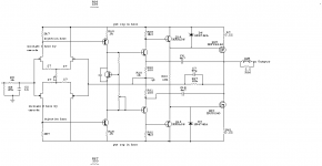
noname,
In your thumbnail (of my primitive design) A1 is in fact the diff'l stage and Vas - it could equally well be a IC op amp with 120db low frequency gain. A2 is the following complementary triple with feedback C - but could equally well be an IC op amp and output stage all in an integrating feedback loop.
Thanks for the threadlink, John. And the simple relationship equation for CMRR/PSRR/load Z and Diff'l gain. of course this applies to a simple op amp model with diff'l pair, Vas,... My more primitive equation applies to the PSRR injection point in whatever topology with A1 prior and A2 after, and particularly relevant to a nested design where A1 may be a complete op-amp with regulated supplies, be it discrete or IC implemented.
Sometimes I think I'm 'out there' alone. Appreciate the backup on the grounded Ccomp Vas.
cheers,
Greg
noname,
In your thumbnail (of my primitive design) A1 is in fact the diff'l stage and Vas - it could equally well be a IC op amp with 120db low frequency gain. A2 is the following complementary triple with feedback C - but could equally well be an IC op amp and output stage all in an integrating feedback loop.
- Status
- Not open for further replies.
- Home
- Amplifiers
- Solid State
- What every Class AB builder needs to be constantly aware of