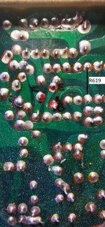
There should be continuity between Q601 base and R619 which means both points have to be at the same voltage.
Identical voltages on R617 and R619 show those points have no current flow. Maybe there is a break in the print around the pad of Q601.
Identical voltages on R617 and R619 show those points have no current flow. Maybe there is a break in the print around the pad of Q601.
im going to break for a bit, but one other thing since my last post R657 to ground has almost 500mv on both sides ,yet C637 has only a few MV's with its connection to C635, so the voltage is coming into R657 from ground, yet there is no current flow across ground
R657 is part of the Zobel network. If the diagram is correct (never assume it is) then the ground connection has to be open circuit. The caps and resistor are a series circuit and so electrically the order of the three of them does not matter so make sure that the resistor really is the part that goes to ground. Electrically it does not have to be, it could be the cap end that goes to ground. So check.
well it is ground if you connect to the tranforsmer grounding, and it is the resistor that is to ground.
you get no continuity if you connect to chassis ground
ive had this before on these amps, and ive often thought of asking this question but never got round to it.
in the attached i have circled in red the grounding point from the transformer on to the filter caps
in green are general to ground references
should these have continuity between them?, because they dont.
They certainly should have continuity. The speaker ground return you circled would always go back to the main reservoir cap ground. All the points do as well but via less direct and heavy (as in thick copper) routes.
So yes, they should all connect together as read on a meter.
So yes, they should all connect together as read on a meter.
Absolutely it could. If that continuity is missing absolutely anything is possible. Things could burn, voltages could be reversed in some parts of the circuit (exploding caps 😉) anything...
An open ground like that has to be something easy. I've never worked on these but make sure grounding does not rely on the board being screwed into place and using the chassis to link certain parts.
An open ground like that has to be something easy. I've never worked on these but make sure grounding does not rely on the board being screwed into place and using the chassis to link certain parts.
well it did make some difference
the diagram says the base should be directly connected to R619 but it isnt, its connected to the emitter, so then im wondering if the transistor is correctly fitted, and if you turn it round so the base is connected to R619, then R631 goes up in smoke.
both transistors have thier collectors as the centre pin so it cant be confused when fitting these ones.
so i got the original transistor out and the config is correct, my new transistor base is as the original, so i put the new one back in and no burning of R613, but i have -1.14v on the base, so its another day without any progress.🙁
but i still have the neg volts issue at the base of Q601, and i just cant work it outAbsolutely it could. If that continuity is missing absolutely anything is possible. Things could burn, voltages could be reversed in some parts of the circuit (exploding caps 😉) anything...
An open ground like that has to be something easy. I've never worked on these but make sure grounding does not rely on the board being screwed into place and using the chassis to link certain parts.
the diagram says the base should be directly connected to R619 but it isnt, its connected to the emitter, so then im wondering if the transistor is correctly fitted, and if you turn it round so the base is connected to R619, then R631 goes up in smoke.
both transistors have thier collectors as the centre pin so it cant be confused when fitting these ones.
so i got the original transistor out and the config is correct, my new transistor base is as the original, so i put the new one back in and no burning of R613, but i have -1.14v on the base, so its another day without any progress.🙁
Its hard to follow with all these different versions and different component references flying around.
Looking at the circuit and I would expect the base to positive by around 600 millivolts or so but the emitter connects to the main output via a low value feedback resistor which is R631 in the diagram above. If the output is negative that will pull the emitter of Q601 more negative and so the base will be pulled down as well. If you have -1.14 on the base then I would expect around -1.8 on the emitter. In other words the base is still around 650mv more positive than the emitter. Measure it and see.
Looking at the circuit and I would expect the base to positive by around 600 millivolts or so but the emitter connects to the main output via a low value feedback resistor which is R631 in the diagram above. If the output is negative that will pull the emitter of Q601 more negative and so the base will be pulled down as well. If you have -1.14 on the base then I would expect around -1.8 on the emitter. In other words the base is still around 650mv more positive than the emitter. Measure it and see.
this is what is strange and i cant work out
Q601
base -1.4v which means it isnt turned on
collector +32v
emmiter +1.5v
with the voltages as they are there isnt many ways the base can become -1.4v
i appear to have a bit of a hybrid version with a bit of all the versions, and that is not helping at all.
i can confirm one thing though, regardless of which version you look at my transistor Q601 is not connected as suggested, and if you do at all goes haywire.
maybe its one of those ones i may never fix.
this is what is strange and i cant work out
Q601
base -1.4v which means it isnt turned on
collector +32v
emmiter +1.5v
Base at -1.4v and emitter at +1.5v tells us it is being incorrectly reverse biased (for an NPN). Just thinking about that and I can't see where the negative value is coming from because the offset trimming is all positive.
You can try this if you want... no guarantees but it is a valid approach. If you remove Q601 and switch on you should have close to the positive rail voltage on where the collector goes. The base should be PLUS something, say 700 or 800mv. That is the voltage across D601. The emitter spot should be at the negative rail because the PNP driver and PNP output will turn fully on via R637 and R649.
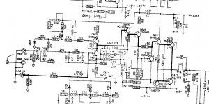
Its worth doing. This is the diagram I'm using for the reference numbers.

Ill give it a try tomorrow
the drawing you have is the one ive been working to, but ive just traced out the back of the board again and the base of Q601 goes to C609, but i will give it a try anyway
remember back to my first few posts and i said R643 was burned, when i put the original transistor c1400 back in, which tested ok, it started to burn again, there has to be something in this
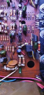
below just shows you the back of the board where Q 601 is and how it is connected underneath.This is the same as the original transistor
sorry about the red pen, but i mark where i am sometimes and clean it off after.

the drawing you have is the one ive been working to, but ive just traced out the back of the board again and the base of Q601 goes to C609, but i will give it a try anyway
remember back to my first few posts and i said R643 was burned, when i put the original transistor c1400 back in, which tested ok, it started to burn again, there has to be something in this
below just shows you the back of the board where Q 601 is and how it is connected underneath.This is the same as the original transistor
sorry about the red pen, but i mark where i am sometimes and clean it off after.
It sounds like there are differences then between what you have and the diagrams. Could C609 and C613 references be reversed?
R643 in that diagram (is that the one you mean?) is a 68 ohm and so what you need to do is look for viable low impedance paths that could be a fault condition.
If Q607 conducts (even if it was shorted) then nothing bad should happen because the output would just rise to the positive rail voltage. That assumes there is nothing connected to the output and that the output and drivers are good.
If Q601 emitter path has a problem then current could be pulled via Q601 through the B-E junction of Q605. Pulling Q601 would prove that. Resistor burns with it fitted, doesn't burn with it removed. C615 and the 0.1uF across it. If they are leaky or have a short then that would do this.
I can't see any other low impedance path that would burn the 68 ohm again that assumes all good with the output and drivers.
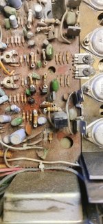
I thought i would spend just a few mins and sit back to look at the difference's in the diagrams.They are all very simlar with very subtle differences.This transistor layout was bothering me when i went to bed last night and i though back to when i first started fixing these things and had transistors that were round the wrong way
so if you look at the attached you will see that 2 different types have been fitted, but they are the same pattern transitor with different pin outs.All the original manufactured parts fitted followed the print pattern,(so shape of part = how to fit it) so if that is the case either one drawing has to be incorrect or the config of the transistor wrong.So i am going to look at and try what you suggested above, and also try a BC 549c in there and see what happens.

so if you look at the attached you will see that 2 different types have been fitted, but they are the same pattern transitor with different pin outs.All the original manufactured parts fitted followed the print pattern,(so shape of part = how to fit it) so if that is the case either one drawing has to be incorrect or the config of the transistor wrong.So i am going to look at and try what you suggested above, and also try a BC 549c in there and see what happens.
so this proves what i was saying about the config first one is the one im working on and have cleaned up, its an early version, the second much later, and dirtier,but with the 549c set up might be usefull later for someone if nothing else
Attachments
The circuit diagrams are electrically viable (the basic configuration is correct). Both are NPN's and the three leads go where they should on the circuit diagram.
2SC type device almost always follow the BCE pinout and BC type usually follow CBE. The BC549C is an old device (very good at the time) but it won't be critical in proving it good. Any small signal NPN of suitable voltage rating should work.
Was the cap that exploded the 1000uF 6.3 volt one below that transistor on the diagram?
yes it was that cap but on the other channel i havent looked at yet(speaker terminal voltage -24v)The circuit diagrams are electrically viable (the basic configuration is correct). Both are NPN's and the three leads go where they should on the circuit diagram.
2SC type device almost always follow the BCE pinout and BC type usually follow CBE. The BC549C is an old device (very good at the time) but it won't be critical in proving it good. Any small signal NPN of suitable voltage rating should work.
Was the cap that exploded the 1000uF 6.3 volt one below that transistor on the diagram?
so it doesnt burn with it removedIt sounds like there are differences then between what you have and the diagrams. Could C609 and C613 references be reversed?
R643 in that diagram (is that the one you mean?) is a 68 ohm and so what you need to do is look for viable low impedance paths that could be a fault condition.
If Q607 conducts (even if it was shorted) then nothing bad should happen because the output would just rise to the positive rail voltage. That assumes there is nothing connected to the output and that the output and drivers are good.
If Q601 emitter path has a problem then current could be pulled via Q601 through the B-E junction of Q605. Pulling Q601 would prove that. Resistor burns with it fitted, doesn't burn with it removed. C615 and the 0.1uF across it. If they are leaky or have a short then that would do this.
I can't see any other low impedance path that would burn the 68 ohm again that assumes all good with the output and drivers.
- Home
- Amplifiers
- Solid State
- wandering centre nad 3020 ser 20