Differential input with current feedback like the INFINITRON with only one CCS (6mA)
No longer the vssa input stage
Do you have an idea for the VAS CCS (16mA) ?
It is difficult to adjust and I have a thermal drift.
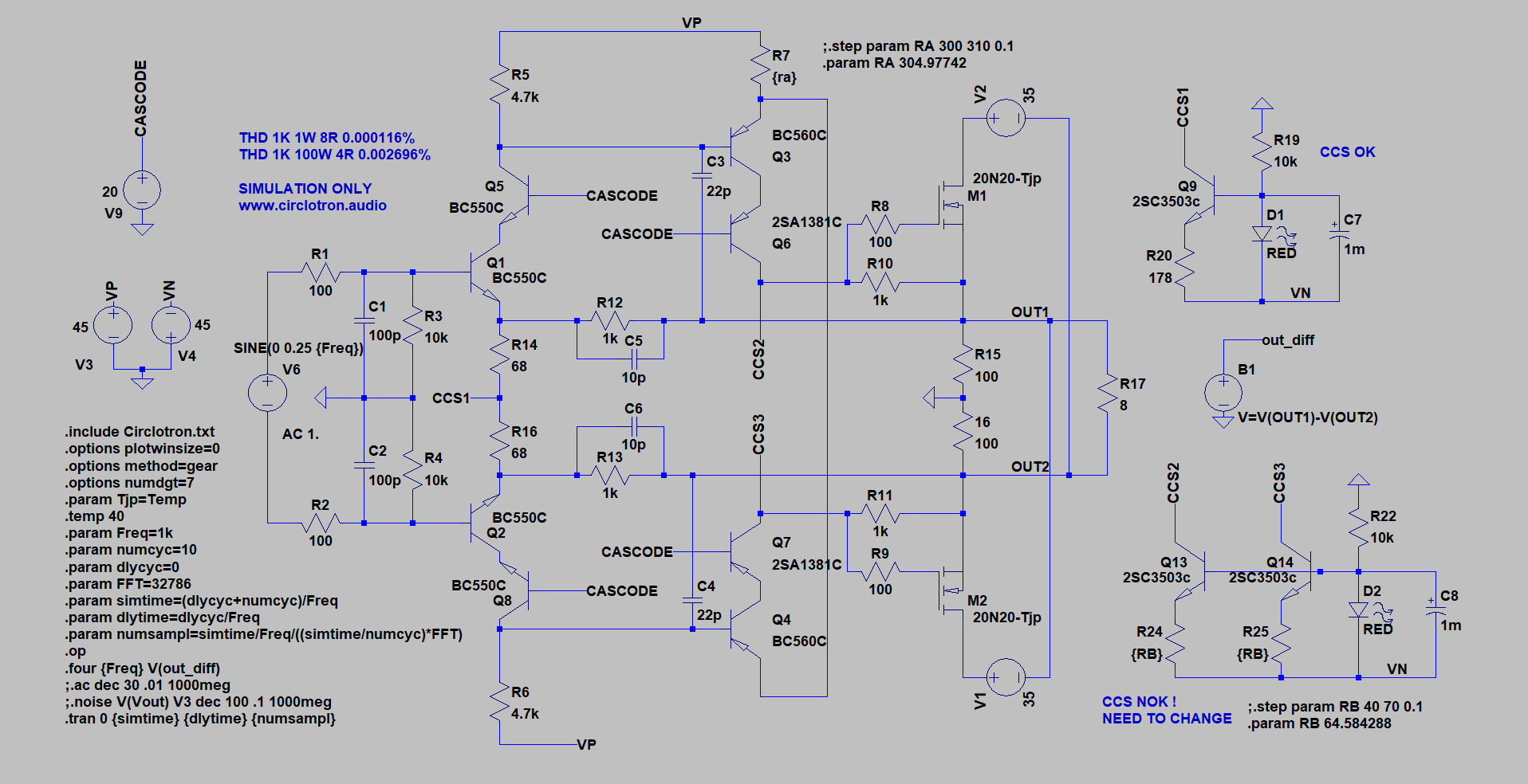
ltspice file
No longer the vssa input stage
Do you have an idea for the VAS CCS (16mA) ?
It is difficult to adjust and I have a thermal drift.
ltspice file
Last edited:
Replace LED with shunt reference and keep voltage across r24,25 at least a volt or so. 2.3 mV/C will yeild +/-57 mV @+/-25C, which over 1 v across Re gives +/-5%. Matched pair may be better choice especially cascoded, but with price tag attached.
Hi UltimateX86,
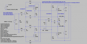
In response to your message, I am replying here as the solution I'd suggest is similar to the one already shown in post #79. Like that circuit, it is a fully floating design, by which I mean it is powered only by the two floating supplies. It also uses no cascodes, as none are really needed here for good performance.
The key difference here is the addition of a differential VAS with active tail current source. This uses a local loop to enhance the differential gain of the VAS, such that even a single-ended input will produce a balanced amplifier output.
The 182 ohm value is adjusted using a trim pot in parallel (not shown) to set the desired output stage bias current. To ensure proper thermal compensation for the bias, the PMOS control device should be of the same process type as the NMOS output stage devices, and mounted near them.
In practice you will need a DC balance adjustment, also not shown. To add this I would first change the JFET drain resistors from 499 to 1K each, and then tie a 2K trim pot across them with its wiper connected to the drain of the PMOS CCS control device.
To be clear, I am offering this for experimental hobby use only. I've not built this exact circuit, but it does sim as expected so I think it will work well in practice. All components and values shown here are what were available to sim and worked for me. You can use what you prefer as long as it works in the end.
If you try this for yourself, I hope you will share your impressions.
Attachments
HI alexberg, thanks i will try with shunt reference (zener?)
Hi Joe,
Thank you for this schema, when I tried this input stage (post 71) I did not use VAS differential yet and the result was not good, maybe because of the 2SK170
so you prefer the J113?
there is not an error in the scheme? the ccs is connected to the input stage and not the VAS
can lateral mosfet be used for better thermal stability?
Last edited:
The schematic is correct as shown, but the approach is a bit unconventional and may require a second look.
It works !!
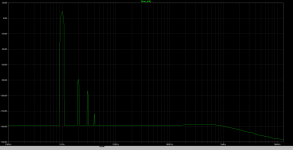
In simulation I found 1mA, 9mA and 300mA, that's what you planned ?
for the moment I took models spice manufacturers, but it would be better in VDMOS with subthreshold to check thermal stability
J113, IRF9520 and IRFP140 are specifically chosen or it could be replaced by others ? (2sk389, irf9610, IRFP240, Exicon lateral mosfet)
Thank you so much !!
Attachments
I gave this reference because I already have some but if you think that the references that you give are more adapted, it is available at mouser so I would take them
Last edited:
Yes, those are about the right idle currents. You can now start replacing the component values with your preferred types and see what works best with them.
Just be sure the JFETs you use can tolerate 24Vds without too much gate leakage (no more than a few mV DC measured at the input), and that whatever PMOS and NMOS devices you use are from the same process type for best thermal compensation.
Thank you for the kind attribution in your schematic. ;-)
Just be sure the JFETs you use can tolerate 24Vds without too much gate leakage (no more than a few mV DC measured at the input), and that whatever PMOS and NMOS devices you use are from the same process type for best thermal compensation.
Thank you for the kind attribution in your schematic. ;-)
to return to Caesar, the input stage come from a Juma circlotron schematic on an other forum that I can not find anymore
https://www.diyaudio.com/forums/members/juma.html
my only interest is to be able to make a circlotron amp
https://www.diyaudio.com/forums/members/juma.html
my only interest is to be able to make a circlotron amp
Hi there Ultimate X86,
Sweet circlotron you got there (this is my favorite topology ever)
Have you tried in LTSpice different output impedance?
Speakers impedance is never linear... And being a CFA topology I'm afraid you'd run into load impedance induced stability problems.
Will also simulate your circlotron once I get home.
Silviu
Last edited:
In practice you will need a DC balance adjustment, also not shown. To add this I would first change the JFET drain resistors from 499 to 1K each, and then tie a 2K trim pot across them with its wiper connected to the drain of the PMOS CCS control device.
Hi,
yes the 499ohm resistor is the best place to control offset, its variation has no influence on the quiescent current (or negligible)
the distortion decreases when increases this resistance, can we increase it?
I tried to increase the quiescent current of the vas, keeping 300mA on output, the distortion increases....
I tried IRF9610, IRFP240, the distortion increases...
Yes, increasing the JFET drain resistance increases open-loop gain and so will reduce the closed-loop distortion, but you may start to see stability issues. The values I chose were a compromise between reasonably low distortion and stability. This is something to watch for when choosing different component values.
The other IRF devices you tried have lower gain than the ones I used, and that is probably why you are seeing higher distortion. You can try increasing the OL gain to make up for it, but there may be a limit, and you may have to add compensation caps for stability rather than rely on the intrinsic PMOS device capacitance (as I did) for internal compensation.
The other IRF devices you tried have lower gain than the ones I used, and that is probably why you are seeing higher distortion. You can try increasing the OL gain to make up for it, but there may be a limit, and you may have to add compensation caps for stability rather than rely on the intrinsic PMOS device capacitance (as I did) for internal compensation.
At first I had a doubt because they are not usual references on this forum, but in this case there is nothing to change, we can build the amp as it is (by adding the potentiometer) ?
I would first try the IRF9610 and IRFP240 in the sim and see how far you can increase the 499 ohm resistor values before you see peaking in the HF response curve or ringing on square waves. There should be none with an 8 ohm resistive load and only a little with some shunt capacitance added. If in doubt, post your results and we can discuss.
Bonjour,
As I said, I have no objection to use J113/IRF9510/IRFP140 but I have to know if it's a good choice, I have never seen an amp with J113 input for example
I hosted all schematic here, it's my public share, anyone can add or remove a file :
Nextcloud
in these schematic there are IRF9610, IRFP240 and the exicon ECW20N20 that I planned to use.
I can not run the amp with exicon 🙁
Last edited:
I still have a question, last week I showed my schematic to Elvee (Circlophone) and he warned me about using mosfets in VAS because of their variation of threshold voltage that had a big influence on the output bias.
So he advised me to use bipolar.
in this new scheme, it is also "sensitive"?
thanks
So he advised me to use bipolar.
in this new scheme, it is also "sensitive"?
thanks
You can use a bipolar VAS if you prefer, but the Vds across the JFETs will go up by a few volts so be careful there. Whatever you use, the PMOS CCS control device will adjust the VAS automatically and, as you saw in your sim, will also thermally compensate the output stage bias.
I have no preference, except :
- ecw20n20, i have 4 selected for Id 280/ 310 with Vgs = 0.5V Vds = 25V
- i have 2Sk389BL and 2sk170 8mA idss
but I have not managed to use them in the schema 🙁
what will it be necessary to do as matching with j113 irf9620 and irfp140 ?
- ecw20n20, i have 4 selected for Id 280/ 310 with Vgs = 0.5V Vds = 25V
- i have 2Sk389BL and 2sk170 8mA idss
but I have not managed to use them in the schema 🙁
what will it be necessary to do as matching with j113 irf9620 and irfp140 ?
in these schematic there are IRF9610, IRFP240 and the exicon ECW20N20 that I planned to use.
In this particular circuit, lateral MOSFETs are not a good choice for the output stage due to their lower current gain vs. vertical types. Use a device that will deliver at least 7A (and more is better) at double its Vgs idle value.
Regarding the input stage, the best choice I can think of right now would be 2SK389 (GR grade is fine), but I don't have a model for it so I used J113.
I dont have GR grade but we could buy LSK389A
.model LSK389A NJF(Beta=37.86m Betatce=-.5 Rd=11 Rs=7 Lambda=4.78m Vto=-0.40 Vtotc=-2.5m Is=35.58f N=1 Cgd=39.9p MJ=0.79 Pb=0.98 Fc=0.5 Cgs=40.7p Kf=0 Af=1 Mfg=Linear_Systems)
.model LSK389A NJF(Beta=37.86m Betatce=-.5 Rd=11 Rs=7 Lambda=4.78m Vto=-0.40 Vtotc=-2.5m Is=35.58f N=1 Cgd=39.9p MJ=0.79 Pb=0.98 Fc=0.5 Cgs=40.7p Kf=0 Af=1 Mfg=Linear_Systems)
- Status
- Not open for further replies.
- Home
- Amplifiers
- Solid State
- VSSA Circlotron