I think there is a problem with the J113, I have an IDSS of 19mA...
nothing in common with 2sk389GR
.MODEL J113 NJF(VTO=-1.2854 BETA=9.25964m BETATCE=-0.5 LAMBDA=3.03839E-2 RD=1.30170 RS=1.30170 CGS=1.05000E-11 CGD=1.20000E-11 PB=5.04493E-1 IS=9.86870E-16 XTI=3 AF=1 FC=0.5 N=1 NR=2 MFG=PHILIPS)
nothing in common with 2sk389GR
.MODEL J113 NJF(VTO=-1.2854 BETA=9.25964m BETATCE=-0.5 LAMBDA=3.03839E-2 RD=1.30170 RS=1.30170 CGS=1.05000E-11 CGD=1.20000E-11 PB=5.04493E-1 IS=9.86870E-16 XTI=3 AF=1 FC=0.5 N=1 NR=2 MFG=PHILIPS)
Attachments
I just tried with bipolar but keeping the CCS vas mosfet, it works pretty well, but better with mosfet.
GND on input CCS is OK in simulation but it is possible with real CCS ?
all files are there
GND on input CCS is OK in simulation but it is possible with real CCS ?
all files are there
Attachments
Last edited:
Hi UltimateX86,
Well, I have tried to keep to the VSSA (very simple) philosophy, but you are forcing my hand a little. ;-)
A real CCS will have trouble with less than 1V across it. If the goal is run the input JFETS at a higher idle current than self-biasing would allow, I would suggest the approach shown below. This uses a battery (or its virtual equivalent) to place the output terminals at a negative voltage that lets more JFET idle current flow through the feedback resistors. This has the added benefit of reducing the Vds across the JFETs, making gate leakage less of a potential issue.
You can certainly use an actual 9V battery for this, as it supplies almost no current and should last for years. Or, you can create its virtual equivalent by adding a 9V zener shunt regulator across each floating supply and combining their outputs through two (say 10K) resistors to charge a single filter capacitor that acts as the virtual battery.
The following diagram only shows this conceptually, as I will leave the implementation up to you. What it does show, however, is that the feedback resistor values have increased to give about 4-5 mA bias through each input JFET. The input devices now see about 14V Vds, so the circuit will now accommodate a wider range of JFET types without problems, and in fact, you can even use NPNs bipolars and enhancement mode MOSFETs as input devices.
As a postscript, you may need to reduce the 499 ohm resistor values in practice with this approach due to the higher input stage idle currents, but I left them as-is in my sim and did not see any stability problems.
Attachments
I would also like to keep a simple diagram, but it's not always easy to achieve, the bipolar schematic was just a POC
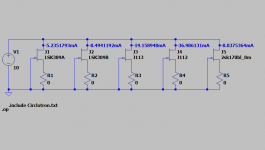
it also works with 2SK170bl, I used the same polarization as the amazing circlotron, 2mA
ltspice files
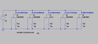
the feedback resistances are a little weak but is this bad ?
I will try with the battery
Thanks for your help
it also works with 2SK170bl, I used the same polarization as the amazing circlotron, 2mA
ltspice files
the feedback resistances are a little weak but is this bad ?
I will try with the battery
Thanks for your help
Last edited:
As a postscript, you may need to reduce the 499 ohm resistor values in practice with this approach due to the higher input stage idle currents, but I left them as-is in my sim and did not see any stability problems.
how do you check the phase margin with a circlotron ?
A simple feedback work also and keep the VSSA philosophy, i have LL1690 for input if needed
Attachments
Last edited:
how do you check the phase margin with a circlotron ?
When predicting stability, it seems to me that circlotrons act much like any other feedback amplifier, so you can use gain/phase plots (assuming your sim provides this), or as I tend to do, just look at the frequency and square wave response with resistive and reactive loads.
The particular design I proposed (with or without the added bias supply) does not require a transformer or other balanced input source, but it will certainly accept one. The distortion residual does change, so if you are sensitive to that, you may notice a difference in sound character.
Using an input transformer (or capacitive input coupling) does give you the option to supply a positive bias to the input stage gates rather than place a negative voltage on the output terminals. This can be useful in cases where having a negative voltage on the speaker terminals is a problem, such as when connecting to an active subwoofer that requires a ground referenced input signal.
HI
I have to deepen the subject "stability" with LTspice, I've never done it
what do you use as a simulator ?
using a simple current feedback like F5 or amazingCirclotron we do not need to add a positive input or negative output voltage
what do you think ?
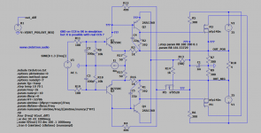
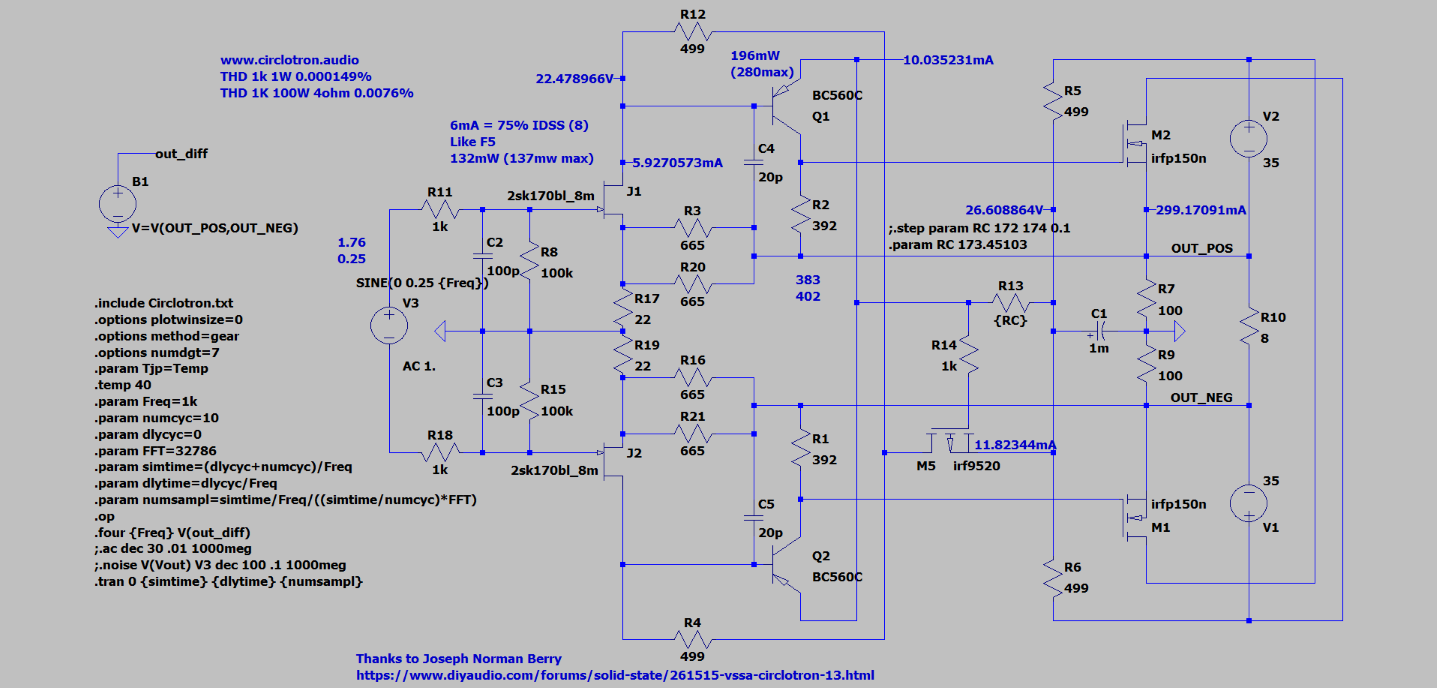
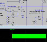
I decrease the supply voltage on VAS to reduce dissipation to be able to use TO92 as you recommended in post 3
you think it's worth using IRFP150n ? (more transconductance but more capacitive)
LTSPICE files
I have to deepen the subject "stability" with LTspice, I've never done it
what do you use as a simulator ?
using a simple current feedback like F5 or amazingCirclotron we do not need to add a positive input or negative output voltage
what do you think ?
I decrease the supply voltage on VAS to reduce dissipation to be able to use TO92 as you recommended in post 3
you think it's worth using IRFP150n ? (more transconductance but more capacitive)
LTSPICE files
Last edited:
Using a simple current feedback like F5 or amazingCirclotron we do not need to add a positive input or negative output voltage. What do you think ?
The F5 and Amazing Circlotron are both wonderful and justly popular class A amp projects, and I agree that simplicity is a big part of their charm. They are also well documented and proven designs, and if you use their specified components, there would be no need for concern over stability issues.
The design I proposed is not an effort to improve on them, but to pursue simplicity in a different context, namely that of a scalable high-performance class AB amplifier topology. The best choice for you may come down to your system requirements, knowledge level, and of course, aesthetic preference.
I do intend to build and document this design when time allows, and it may then become a more attractive DIY option to consider.
I simulated your amp, the original with j113 at 1mA and actually it's stable on 1khz 4V square with 1uF on load
mine is a super oscillator 😛
when you build it will be with the j113 to 1ma and irf9520 ?
mine is a super oscillator 😛
when you build it will be with the j113 to 1ma and irf9520 ?
Attachments
Last edited:
Is it the circuit in post #150 that is oscillating? If so, it may help to move the compensation caps. For example, you can try from collector to base of each Vas transistor, or from each Vas collector to the source of the JFET driving it.
Nothing wrong with using the self-bias connection shown there, as long as you don't mind a little DC on the output, which fortunately also lowers the JFET Vds a bit. And I think you'll still be able to drive the amp input single-ended if you want.
Nothing wrong with using the self-bias connection shown there, as long as you don't mind a little DC on the output, which fortunately also lowers the JFET Vds a bit. And I think you'll still be able to drive the amp input single-ended if you want.
Is it the circuit in post #150 that is oscillating? If so, it may help to move the compensation caps. For example, you can try from collector to base of each Vas transistor, or from each Vas collector to the source of the JFET driving it.
Nothing wrong with using the self-bias connection shown there, as long as you don't mind a little DC on the output, which fortunately also lowers the JFET Vds a bit. And I think you'll still be able to drive the amp input single-ended if you want.
Hi,
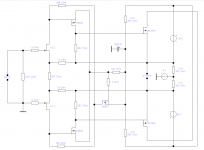
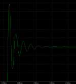
Yes it is the #150, so i try 47P on Jfet source to collector, not good.
47p on base to collector seems to work, that's enough?
In fact i have a balanced output Dac/preamp so I would like use XLR on amplifier input
what I use in balanced input is good or not ? (1k 100k 100p)
thanks
Attachments
Last edited:
Ideally you want minimum overshoot and ringing on reactive loads. I'm not aware of any standard for this, but I like to see no more than 20% overshoot followed by no more than 1-2 cycles of damped ringing, like the results you saw from the circuit when using my component values.
You might see improvement with your bipolar Vas by adding a resistor in series with each Vas emitter. I would try values in the 10-100 range and see if that improves square wave response. You may still need the collector-base caps, but I'm not so sure about the ones shunting the inputs.
You might see improvement with your bipolar Vas by adding a resistor in series with each Vas emitter. I would try values in the 10-100 range and see if that improves square wave response. You may still need the collector-base caps, but I'm not so sure about the ones shunting the inputs.
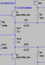
I put the j113 but with an higher current with 100ohm in parallel to keep E92 series
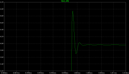
0 overshoot
http://circlotron.audio/data/simulation/img/20190527_J113.png
http://circlotron.audio/data/simulation/img/carreJ113.png
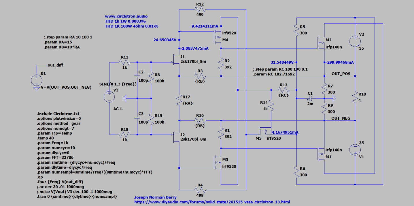
I also noticed that increasing R7 R9 decrease the distortion without changing the bias point, i keep 300ohm ?
0 overshoot
http://circlotron.audio/data/simulation/img/20190527_J113.png
http://circlotron.audio/data/simulation/img/carreJ113.png
I also noticed that increasing R7 R9 decrease the distortion without changing the bias point, i keep 300ohm ?
Last edited:
I put the j113 but with an higher current with 100ohm in parallel to keep E92 series
0 overshoot
http://circlotron.audio/data/simulation/img/20190527_J113.png
http://circlotron.audio/data/simulation/img/carreJ113.png
I also noticed that increasing R7 R9 decrease the distortion without changing the bias point, i keep 300ohm ?
The step response looks like it has some high frequency ringing. Try a freq sweep from 1 Hz to 50 MHz. In a real build, I have found these high freq peaks in gain. From the spacing of the peaks of ringing, I guess 2MHz.
Last edited:
- Status
- Not open for further replies.
- Home
- Amplifiers
- Solid State
- VSSA Circlotron