Hello,
Apparently the moderation has stopped just after my previous message, because I found out that now I can send PMs again. 🙂
Kind regards,
Kees.
Apparently the moderation has stopped just after my previous message, because I found out that now I can send PMs again. 🙂
Kind regards,
Kees.

Yeah, I saw it, not too late, I hope 🙂
Took a few stabs in the dark, i.e. purchasing "random" Japanese magazines from 197x 😀, but...I will go back to Ditratherm story in post #63.
I saw that info in one document originated in Asia, which looked reasonably credible,
and, of course, requiring investigation.
Recently, I have clarified the origins of the V### V-FETs - it is from NEC - their development
parts numbers (for the registered 2SJ19_20_21 / 2SK69_70_71).
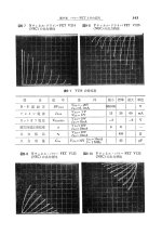
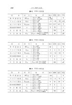
I will attach the comments from someone in Japan, who quoted one document from the summer
of 1974, (clearly from Japanese magazine).
Attachments
@ilimzn and others
Any idea what the CRSS (reverse tranfer capacitance) looks like for the K60 and J18?
I wonder how it compares to CRSS of lateral mosfets (see example).
https://www.exicon.info/PDFs/ecx10p20.pdf
Any idea what the CRSS (reverse tranfer capacitance) looks like for the K60 and J18?
I wonder how it compares to CRSS of lateral mosfets (see example).
https://www.exicon.info/PDFs/ecx10p20.pdf
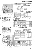
Scratch these off the list - while they are high voltage (but JFET, not SIT), their curves are nothing but pentode-y dreariness... 😛Also, there was rumor in Japan that Shindengen made UN01 as a SIT (TO-39 case) in the
mid '70s...
View attachment 1041649
Attachments
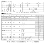
Hey @Soundhappy, anything about these in your datasheets?Probably TM series are triodes but TBM are pentodes.
Transistors pair or quad in one case
It looks like an IGBT module for power inverter, for sure it is vfet
(shown on the label), but its input capacitance is at least 10-15nF.
Even more.
(shown on the label), but its input capacitance is at least 10-15nF.
Even more.
yes, the format looks like an IGBT, but it is the same as that shared by @Soundhappy.
and yes, definitely a dual vfet according to my tracer pulse check:


also thinking we are correct about more than a few nF of input capacitance.
and yes, definitely a dual vfet according to my tracer pulse check:
also thinking we are correct about more than a few nF of input capacitance.
Can you measure it? (the Ciss)
I tried to simulate 2 stages single ended class A, a voltage gain stage with 2SK79, and a source follower
with 2SK82, loaded with constant current source with IRFP240, the result was much worse than the other
variant with LMOS ECX10N20 (2 in parallel). I also tried with 3, even 4 2SK82, but without any significant
success. VFETs (and triodes) will work much better when their load is connected to anode/drain, instead of
cathode/source. Their triode characteristics are not usable when they work as a follower, any good linear
transistor performs better, as its inner resistance is much lower and its linearity is not so important when
it works as a follower.
Last edited:
Eventually will get to learn more about them.
As far as using them for their triode characteristics , I would stick to something tried and tested

Yamaha b-1 harmonics profile.
As far as using them for their triode characteristics , I would stick to something tried and tested
Yamaha b-1 harmonics profile.
Good evening DIY friends,
Got curious/ greedy and ordered some 2SK183 from ebay. Need help in seeing if these are legitimate or not. I have measured with my daughters school ruler.


Got curious/ greedy and ordered some 2SK183 from ebay. Need help in seeing if these are legitimate or not. I have measured with my daughters school ruler.
use Calipers or at least metal ruler, these are much more precise than plasticky thingies for school fun

The very crude measurements that I took checked out. The skirt measures 55. Drain measures 30. The source measures 43.

As far as testing, I have someone willing to curve-trace them for me. I'm just trying to ensure that they are real before I send them his way, not to waste his or mine.
The only thing that I am unsure about at this point is the lettering. Usually, most I have seen only have Tokin on one side and the part number on the other, this one has it together. It looks like a newer part...
bigger circle plate is Drain, smaller is Source, wire is gate
though - hoping they're real deal, good luck with heatsinking arrangement
using Keratherm 86/82 as pad for drain, same for source, I should go with squeezing it between two heatsinks
or if luck is on your/our side, maybe it's possible to use just one side heatsink - for Drain; then it can be clamped with - say - proper plate made of aluminum sheet (at least 3mm thick) isolated with piece of bare pcb material
that, not going above, say, 100W of heat per device
for more, I would go with non-isolated direct contact, heatsinking on both sides ..... which means heatsinks isolated from chassis
all that, trying to recall in memory few pics of same ones in some industrial assembly ......... I believe it was Soundhappy who posted those
Oh boy... instead of getting my Furious amplifier builder badge.. more like a foolish amplifier builder badge.
It should be fun, If I don't screw it up somehow....
So essentially I have two live heatsinks, one for the source and the drain?for more, I would go with non-isolated direct contact, heatsinking on both sides ..... which means heatsinks isolated from chassis
It should be fun, If I don't screw it up somehow....
or if luck is on your/our side, maybe it's possible to use just one side heatsink .......
that, not going above, say, 100W of heat per device
that I meant - with Keratherm sheet as isolator; need to be confirmed with proper measurement, allowing no more than 10C of difference between drain plate and heatsink ditto to drain body
and .......... I wouldn't go without hefty follower as driver, say 30mA of Iq or more
- Home
- Amplifiers
- Pass Labs
- vFET / SIT data sheets