Hi Lee,
If your actual build is in line with the schematic, and if I did the calculation right, the CCS seem to be sourcing/sinking about 36mA.
In a diamond buffer like yours, it appears to me the driver transistors need to have a Vbe smaller than that of the output transistors by a certain margin in order to operate at a certain, sufficient level of quiescent current. Emitter degeneration at the output transistors can help biasing the driver transistors if the drivers' Vbe is higher than what is desired, but in the application in question you don't want to increase that degeneration. So a driver transistors having a suitable Vbe seems to be a must.

On the other hand, if the output transistors have a known Hfe at 100 or less, and they are operating at 3.7A as your earlier post hinted, they would have taken all those CCS supplies as their base current, and left nothing to the driver transistors. That, to me, seems to be suggesting the drivers are not being biased sufficiently -- you should be seeing CCS surplus from output transistors' Ic/Hfe, but you don't.
If your actual build is in line with the schematic, and if I did the calculation right, the CCS seem to be sourcing/sinking about 36mA.
In a diamond buffer like yours, it appears to me the driver transistors need to have a Vbe smaller than that of the output transistors by a certain margin in order to operate at a certain, sufficient level of quiescent current. Emitter degeneration at the output transistors can help biasing the driver transistors if the drivers' Vbe is higher than what is desired, but in the application in question you don't want to increase that degeneration. So a driver transistors having a suitable Vbe seems to be a must.
On the other hand, if the output transistors have a known Hfe at 100 or less, and they are operating at 3.7A as your earlier post hinted, they would have taken all those CCS supplies as their base current, and left nothing to the driver transistors. That, to me, seems to be suggesting the drivers are not being biased sufficiently -- you should be seeing CCS surplus from output transistors' Ic/Hfe, but you don't.
Hi nattawa,
I don't know how to calculate the current of a CCS by hand, but simulation says this should be 105mA and this is also what I measured on the bench.
You are right, there seems to be an issue with starvation of something.
I did some simulation and found out that this is related to the filter R12 / C2. Increasing the value of R12 starves the driver.
This seems related with what you also mentioned: Vbe of the transistors. There is only a super small margin by the OPS degeneration resistors. I guess that once there is some current flowing through R12, the driver transistors Vbe is starved.
Next experiment would be to remove the filter R12 / C2 entirely. Maybe the issue is gone then.
Ronaldo asked for simulation files. The file is a mess I'm currently cleaning up a bit and may post before I leave.
Here is the driver and OPS simulation file illustrating the issue in transient analysis.
Attachments
Hi Lee, I must confess I was not paying attention and made a mistake in working out the CCS current from the schematic by missing out one of its two paths -- I should have doubled what I thought to be the CCS current. So my calculated CCS current should have been 36 * 2 = 72mA. That was base on 2.4V Zener diode voltage drop.
The voltage drop over the Zener diodes at the operating current in the simulation is a lot higher than 2.4V, at 3.16V, so we are seeing very healthy 100mA CCS current. Your build matches that quite well.
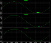
The driver current plot in transient analysis shows no signs of starvation. Yet it does show the current discontinuity in the driver transistors when higher resistance R16 is in use.

The Vce plot of Q39 shows the driver transistor goes into saturation at R16 = 100 ohm. It's cascoded collector gets too much voltage drop over R16. (in the plot the Vce is blown up 10x for visibility)

The R16-C1 seem to need some special attention to keep the driver transistors from saturation under all valid audio signal conditions, plus some good margin.
The voltage drop over the Zener diodes at the operating current in the simulation is a lot higher than 2.4V, at 3.16V, so we are seeing very healthy 100mA CCS current. Your build matches that quite well.
The driver current plot in transient analysis shows no signs of starvation. Yet it does show the current discontinuity in the driver transistors when higher resistance R16 is in use.
The Vce plot of Q39 shows the driver transistor goes into saturation at R16 = 100 ohm. It's cascoded collector gets too much voltage drop over R16. (in the plot the Vce is blown up 10x for visibility)
The R16-C1 seem to need some special attention to keep the driver transistors from saturation under all valid audio signal conditions, plus some good margin.
Last edited:
After taking a break for some time, I picked up this project again.
I figured out that there is probably nothing wrong with the diamond buffer output stage once R12 is low enough and C2 removed. I blindly coped this from Bob's design. This filter might work well in the original application Bob had in mind, but just doesn't seem to be a good idea in my application. For the time being, I also dropped C3 to be sure it doesn't get in the way finding the root cause of the oscillation.
I found out that the front end is the root cause for the oscillation, likely because the miller input compensation is not optimized.
The oscillation frequency is roughly equal the unity gain crossover frequency, which indicates that the miller compensation loop is not properly compensated.
I set the unity gain crossover pretty low to be on the safe side (~600kHz), but obviously this didn't help to get it right easily.
I experimented with optimizing the compensation and found that this is difficult in simulation.
In simulation, the amplifier seems to be more or less stable all the time regardless of how I tune the six components involved in compensation.
In reality, the setup optimized in simulation oscillates terribly on the bench, while the best working bench setup simulates terribly.
Right now I have:
R80=1k and C80=100pF
R81=340R and C81=22pF
R83=300R and C83=150pF
This works with the feedback taken from the speaker output and shows only small overshoot and a bit of well damped ringing in the square wave response.
Simulation and gut feeling suggest C83 should be 47pF, but this doesn't work in reality.
Increasing R80 has helped a lot, which I find a bit counter-intuitive.
Decreasing R81 didn't make any difference.
Decreasing C83 would dramatically improve phase and gain margin in simulation, but unfortunately does not work in reality.
Unfortunately, I didn't find any resources that really help to get the miller input compensation right.
Bob briefly explains the basics in his book and mentions that it is difficult to compensate the miller loop and takes a good deal of experimentation and simulation.
Does anybody have experience with miller input compensation or know any resources that might be helpful?
Does anybody know how to approach simulating the stability of the miller loop (sorry for asking)?
I did some research already, but found surprisingly little information about MIC.
MIC doesn't seem to be the most popular compensation technique, probably due to the complexity and many appealing alternative compensation schemes.
Here is the best advice I found so far:
Miller Inclusive Compensation (MIC) Design Example
But I'm having difficulties following the discussion.
Miller Inclusive Compensation (MIC) Design Example
But I'm having difficulties following the discussion.
Bob explained an approach for calculating MIC here:
Bob Cordell's Power amplifier book
I haven't found this earlier and will try to follow the procedure.
Bob Cordell's Power amplifier book
I haven't found this earlier and will try to follow the procedure.
Finally I succeeded stabilizing the amplifier using the shared experience I found here on DIY Audio.
First I will explain how I stabilized the amp and later I will collect everything that helped me so that anybody trying to stabilize an amplifier using miller input compensation might enjoy this more than I did.
The biggest step towards a stable amplifier was lowering the gain from 40 to 20. I can't remember why I set the gain so high. This project is ongoing for years now with breaks in between of months and years. Sometimes it is as if a stranger designed my circuit and I just wonder about all the questionable design decisions.
With the gain set to 20 like in Bob's amp and book, everything makes much more sense.
I figured out, that by lowering the gain, I can keep the miller cap at 22pF and that the resistor in series with that cap is best at roughly 680 Ohm as proposed. I chose 750 Ohm. This results in a unity gain crossover frequency of roughly 900kHz in my case. Note that the other compensation components also influence the crossover frequency (to lower).
The shunt at the output of the VAS is recommended to have the same time constant like the miller cap and the resistor in series with it. I chose the shunt cap to be 100pF since a higher value has helped previously when the gain was higher. Bob recommends 50pF, but also has observed that higher values may contribute to stability in certain cases. With the shunt cap being 100pF, the shunt resistor in series would need to be 165 Ohm. I chose 150 Ohm because this is the closest value I have at home.
With four of the six compensation components set, the lag compensation of the LTP can be optimized. I started with 150pF and a few hundred Ohm and experimented until I found the optimum values. This was outright unstable.
I quickly found out that the resistor should be much higher in my case than in the examples. The zero formed by the resistor seems extremely important for stability. 1kOhm was not enough and I settled for 1k5. The effect of the resistor is clearly visible in simulation. Neither too low isn't good, nor too high.
The effect of the capacitor isn't obvious from the simulation I did. Maybe this is because I'm not really good at simulating circuits. The higher, the more stable, but once a certain value is exceeded, stability is lost again. I didn't try a larger cap than 330pF.
The tricky point is well visible from the loop-gain plot. At roughly 4Mhz, where the phase drops quickly, there is a tendency for a gain peak to occur. It is difficult to find a proper balance of the components compensating the miller loop to not create a gain peak here.
What makes MIC so complicated to optimize is that so many components are involved. A seemingly infinite number of combinations can yield the same (apparently stable) result, which is not stable in reality.
I think the best order to set component values is:
1. The miller cap
2. The resistor in series with the miller cap
3. The shunt resistor at the VAS output (with the shunt cap being a fixed value of maybe 50 to 100 pF)
4. The compensation of the miller loop in the LTP
Once the amp oscillates, there is smoke for sure and it takes less than a second after onset of oscillation to show up.
Oscillation at ~500kHz does not do as much damage as oscillation at ~4MHz.
With the gain set to 40, the oscillation occurred at ~500kHz and with the gain set to 20, I mostly had oscillation at maybe 4MHz (couldn't measure that quickly).
Once the amp started to oscillate, the oscillation was persistent until I pulled the plug.
I burned several 15Ohm resistors at the loudspeaker output shunt (R51 and R52 in the OPS schematic). Meanwhile I replaced the two parallel 15Ohm resistors by one 10Ohm 4Watt metal oxide resistor I found in the resistors box. The output inductor apparently does not save the shunt at the loudspeaker terminal from high frequency.
I haven't understood yet why I also burned several ground breaker resistors (R1 in the front end schematic). Maybe this has saved other components from burning down.
At the moment, the amp is pretty stable, showing only a bit of overshoot at the square wave corners, and tolerates some capacitance as (only) load connected after the output inductor. I tried 33nF, 100nF, 1uF and 2.2uF and there is just a bit more overshoot at the corner of the square wave.
In simulation it is tolerable to connect up to 100nF as load prior to the inductor.
So far, I'm pleased and will investigate how to further tweak the circuit for better performance.
Attachments
Last edited:
Here is a collection of posts that I found very helpful. Some of the post are a bit out of context, but you will find the context following the link to each.
Hi Glen,
Here's how I do it. Let's assume I've chosen a closed loop gain of 20 and a gain crossover frequency of 2 MHz. This means that I want the forward gain of the combined input stage and VAS to be 20 at 1 MHz, assuming that the output stage has unity gain (if the output stage had a gain of 2, the target would be 10 instead). Having chosen the feedback shunt resistor to be 215 ohms, I now know that the reactance of C4 must be about 19 times 215 ohms at 1 MHz, or about 4k. Thus c4 becomes 20 pF.
I then want to put in a stabilizing zero at a frequency above the gain crossover frequency. This is done with R13 at 680 ohms. This gives me a zero at about 11 MHz.
Next I analyze and stabilize the inner loop that is closed by C4 and R13. This can be a high-bandwidth loop with a gain crossover beyond 10 MHz, since only small-signal fast transistors are in the loop. This fast loop is stabilized by C3 and R14. This is very light lag compensation.
Note that there is not a lot of interaction at the base of Q2 because the 215 ohm resistor is small compared to the impedances of C4 and R12.
The advantage of the scheme is that it rolls off the high frequency forward path gain by applying feedback around the input stage, increasing its dynamic range, reducing its distortion, and not making it work harder at high frequencies (the way Miller compensation does). It only has to work harder at very high frequencies where C3 comes in, but this is pretty far out.
This compensation approach is what allows me to get 300 V/us slew rate. It is like input compensation in a way, but is more elegant because it does not use the brute force of shunt lag compensation across the input gates.
Cheers,
Bob
Hi Rafael,
Sorry to be so slow in getting back to the issue of determining MIC compensation component values.
Mike is right about the MIC minor loop stability. It must be taken into account and evaluated. This can be done by breaking the loop right at the input to the LTP. At that point, the contributions from the MIC compensating capacitor and the output of the amplifier will have merged and summed.
Interestingly, the ULGFs of the major and minor loops are so far apart, perhaps a decade, that the major loop feedback contribution to the minor loop gain of the MIC is pretty much inconsequential in the frequency rangle of the minor loop ULGF.
Compensating the MIC minor loop can be tricky because there are so many possible combinations of the resistance and capacitance values. However, a simple rule-of thumb approach can be used to converge on a circuit fairly quickly. As shown in Figure 9.7 in my book, there are three R-C pieces to the design. The first is C1, the MIC dominant pole compensation capacitor against feedback resistor R2 and feedback shunt R1 (ignore R3 for now and let it be zero, as it often can be). The global ULGF is set by making C1s reactance equal to R2 at the desired global ULGF.
The second R-C piece is the IPS shunt lag-lead load consisting of C2 and R4. This is the primary compensation network for the MIC loop. For now, you can assume R4=0.
The third piece is the VAS R-C load consisting of C3 and R5. In some designs you can get away without it, but I strongly recommend it. It establishes a predictable and dampening load for the VAS at high frequencies. It also controls what proportion of the VAS signal current flows back through C1. Indeed, for most designs you can arbitrarily set C3 to 50pF. If you make it too big, you will impair the achievable slew rate of the VAS. Now, select R5 to set the time constant of C3*R5 to be the same as the time constant of C1 and the resistance it has in series with it. The division of VAS signal current between the two paths (through C1 and C3) will now be largely flat with frequency.
Now just set the value of C2 (I just do it by simulation) to achieve the desired minor-loop ULGF. I usually choose about 10MHz. Optionally add some resistance at R4 to optimize phase and gain margin of the minor loop. Resistance can be added at R3 to add some phase lead to optimize the global gain and phase margin, if desired. If resistance is added at R2, one may wish to appropriately revise the value of R5. Note that even with R3 = 0, the non-inverting amplifier structure of the MIC loop prevents its gain from going below 0dB, so a zero is created there no matter what.
Finally, note that the values in Figure 9.7 do not obey this design approach. While that design is quite stable, I don’t think it is optimal.
Cheers,
Bob
Hi Rafael,
(...) keep in mind that R1 and R2 comprise the feedback network that would be there with any kind of compensation.
With R3=1k, the forward open-loop gain of the compensated amplifier cannot go below +6dB (i.e., X2) in theory. If the closed loop gain of the amplifier is 20, and ULGF is 1MHz, the zero will occur where the closed loop gain will have fallen to 6dB at 6dB/octave. This will be one decade above 1MHz, i.e., 10MHz.
I've not bothered to do the math to calculate the needed value of the LTP shunt capacitor to achieve the desired ULGF of the minor loop; I just adjust it by simulation.
Cheers,
Bob
Hi Mike,
You make a good point. I'll check it out with some simulations. This is definitely an issue that I should address head-on in the second edition. In a number of cases I have been using a series R-C shunt on the VAS output node (even when not using MIC). Indeed, it has often been on the order of 100pF and maybe 100+ ohms.
I have also had some suspicion that issues like this have been partly involved in the instability of Triples that some have seen.
More recently, I've seen some interactions where I used a helper transistor on the IPS current mirror load. This was in cases where I used a VAS preceded by an EF and a Triple output stage.
One of the things, possibly related to all of this, that I have been looking more closely at is gain margin. I have seen numerous cases where there is above-band peaking in the closed-loop response. While this does not necessarily suggest dangerous instability, it can be a troubling wake-up call. 6dB of gain margin is often safe enough against oscillation, but it takes about 10dB of gain margin to have a monotonically decreasing closed loop response above the ULGF. Interestingly, in most cases where I have enforced a 10dB gain margin, phase margin was well over 60 degrees.
This underlines the need for people to measure the closed-loop response of modern amplifiers up to at least 10MHz.
(...)
Cheers,
Bob
I agree, If there is peaking in one of the local loops, it can cause peaking in the overall open loop gain, and this will inevitably result in peaking in the closed loop gain at frequencies above the ULGF.
However, and importantly, even if you have a perfectly done front end with no instability in any local loops it might have, you can also get peaking in the closed loop response above the ULGF if the amplifier has smallish gain margin. This can happen, for example, as a result of poles adding additional lagging phase in the output stage. For example, a 6dB gain margin will result in such a peak even without any local loop instability or peaking.
So there are two possible causes of closed loop peaking above the ULGF.
For purposes of this discussion, what I mean by closed loop peaking as any non-monotonic fall-off in closed loop gain above ULGF.
I like your assertion that if the closed loop gain looks OK, then the internal loops are OK. I have been leaning toward this very same assertion. If true, it is a profoundly useful observation because it is so easy to check in the lab.
Can we agree that "OK" for closed loop gain means a monotonic fall-off of closed loop gain above ULGF?
If so, and we follow this rule of thumb, there may be some cases that result in amplifiers with overly-conservative compensation as viewed by some, but it is wise to err on the conservative side, especially given the degradations that may occur in real-world situations. For example, we may have lots of amplifiers with gain margins of 10dB or more and phase margins of 70 degrees or more, but so be it.
Cheers,
Bob
Hi Glen,
I think I agree with your analysis with regard to that implementation of what I refer to as input Miller compensation. The need to compensate the Miller loop does have a cost, and I believe it can have this modest sticking effect you show. It looks like in the case you presented, the sticking interval is about 1 us.
I don't like sticking at all, although this amount and kind of sticking seems more benign that a lot that I've seen, especially when any transistors are allowed to saturate. Of course, sticking will be influenced in different amplifiers depending on whether the VAS or the output stage clips first, and whether or not Baker clamps are used.
I have not looked closely in simulation recently at my MOSFET amplifier to see how much of this type of sticking behavior it exhibits. However, there is no question that your observation about the Miller loop compensating capacitor attaining a charge during clipping that must be dealt with during a sticking interval is true. Its just a matter of how long this interval will be.
This compensation scheme thus does have a cost, but it does also have big benefits in terms of naturally-achievable slew rate (300 V/us in my amp) and the fact that it effectively encloses the input stage in a feedback loop.
In later implementations of my compensation scheme, I've added a series R-C shunting the VAS output node to ground as part of the Miller loop compensation. In some designs this improves the stability of the Miller compensation loop. In some cases, the use of this R-C allows one to decrease the size of the LTP shunt capacitor, reducing the sticking. Another key point to keep in mind is how high the allowable gain crossover frequency for the Miller loop can be. Obviously, the higher we can make it, the smaller need be the capacitance shunting the LTP.
One other thing to bear in mind is whether a resistor is inserted in series with the main Miller compensation capacitor (providing a zero in the open-loop response above the gain crossover frequency). This can have an influence on the necessary compensation for the Miller loop.
BTW, I have also seen really excellent results with TMC. I have also applied TMC back to the LTP inverting input with success.
Cheers,
Bob
While the square wave tests looked promising, there probably was a mistake in the setup: Due to a soldering issue, the loopgain was collapsed significantly. I can't remember exactly when I found this out.
Also, square wave input was only 0.3Vpp so with a gain of ~20, this was not a large output voltage.
When I proceeded to sine wave testing at higher volume, I discovered a lot of instability that plagues me for many weeks now.
Meanwhile I replaced all resistors involved in the compensation with trimpots in order to quickly change compensation.
An important omission in the first design was the R-C shunt at the node where the clipped signal is conducted to. I added this to the assembly and it improved stability during clipping.
I also replaced the driver transistors (TTA/TTC) by BD139 / BD140 because I believe they are better suited in such extremely low Vce applications.
However, I'm still far from a stable amp.
Please find attached simplified LT Spice file in case you like to play with the circuit. This is currenly a mix of what I built and what I plan to improve in the next revision.
In simulation, the amp is still easy to get stable and performs well. Reality disagrees.
Even worse, reality is the exact opposite: Setups that should be totally unstable in simulation work somewhat well in reality and vice versa.
Attachments
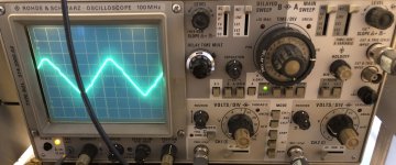
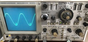
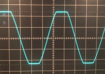
Here are some screenshots of clipping.
What I find odd is that the positive clips earlier despite the clipping references being exactly same voltage.
The worse picture was taken during power up. This shouldn’t look worse because according to simulation, the amp powers up well behaved.
What I find odd is that the positive clips earlier despite the clipping references being exactly same voltage.
The worse picture was taken during power up. This shouldn’t look worse because according to simulation, the amp powers up well behaved.
Attachments
Great to hear that somebody is actually interested in my project.
Sometimes I feel like spamming the forum with my stupid stuff.
I understand that I don't receive many replies since it is difficult to help me with issues that might not be present in simulation.
Today I tried something and figured out something:
I increased the Miller capacitor dramatically to see how much it would take to get rid of the oscillation.
Maybe 47pF would have been enough, but at 100pF and the potentiometers optimized, it is almost stable now.
When I put the numbers into simulation, I saw that not only the unity gain crossover frequency has dropped to ridiculously low 300kHz, but now something became visible that was hidden before: A gain peak at 3-4MHz. This is where the phase turns -180°.
This gain peak probably has been there all the time, but was covered by much higher ULGF before.
Since the amp still has a tendency to oscillate despite brutal knock-down compensation resulting in huge phase margin, I suspect that the gain peak is the reason for instability. Even in simulation, gain margin is not good right now. This gain peak might be even higher in reality.
I stumbled across a project with somewhat similar experience:
Open loop gain peaking
This could be resolved in the end.
One thing is for sure: I need a larger Miller cap with such a large output stage. Bob used a single pair of power transistors and I use four pairs.
I hope I can figure out how to tame the gain peak and have a Miller cap of maybe 33pF with ULGF of maybe 800kHz in the end.
I still have a lot of emitter degeneration in the first LTP that I would like to get rid of. In simulation, high emitter degeneration in either LTP worsens gain margin considerably. I have no idea why.
I reality, lowering the degeneration increases instability.
Right now I'm not sure which issue to address first: The positive clipping that should not be there or the instability. Both may be related. Already triple checked assembly and what I put on the board equals the schematic. Simulation doesn't show any asymmetric clipping.
Attachments
Last edited:
I haven't been in my "lab" this week, but made up my mind a bit.
Last thing I tried was to lower first LTP degeneration to 200R and miller cap to 47pF. Stability seems unaffected.
The amp in general seems stable during normal operation. Instability only occurs during clipping.
I simulated the circuit again to figure out what could be the problem.
The compensation of the clipped feedback path could be insufficient. Adding a shunt R-C network to this node (like the VAS output has one) helped a lot already. Do I need another Miller cap to compensate clipped feedback as well? If so, how to wire this then? I have C84 and R84 across the diodes in the feedback network that could be helpful. Probably I will keep them on the next revision of the PCB.
I observed the most dramatic effect in simulation by increasing the base stoppers for Q18-Q21. Currently I improvised base stoppers here with 4.7kOhm, which does not seem enough. Simulation shows that 10k base stoppers would be required.
I don't really have an idea why those base stoppers improve stability during clipping.
This is what I'm going to experiment with next week.
Attachments
My prototype of the front end with all the improvised changes and additions increasingly fell apart during experiments and I decided to continue with a new PCB revision that includes all changes I improvised plus some small improvements.
Among the improvements are more compensation options like simple Miller compensation, TPC and BTC.
There is a trimpot option for most resistors of the compensation network. This is really fun to experiment with.
I also went back to simulation and figured out that MIC with less than 47pF Miller capacitor won't work with that powerful output stage.
TPC / BTC looks very promising, allowing me to lower UGLF in order to maintain stability with the huge OPS and a lot of NFB at 20kHz.
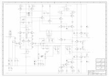
Attached is the schematic of the revison 2 board.
Among the improvements are more compensation options like simple Miller compensation, TPC and BTC.
There is a trimpot option for most resistors of the compensation network. This is really fun to experiment with.
I also went back to simulation and figured out that MIC with less than 47pF Miller capacitor won't work with that powerful output stage.
TPC / BTC looks very promising, allowing me to lower UGLF in order to maintain stability with the huge OPS and a lot of NFB at 20kHz.
Attached is the schematic of the revison 2 board.
Attachments
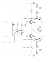
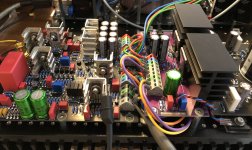
Since I could not figure out whether the front end or the driver stage is to blame for all the weird instability, I also designed a different driver stage.
This is a pretty textbook like diamond driver stage, that forms a diamond buffered triple together with the output stage.
The CCS output 10mA.
This is a pretty textbook like diamond driver stage, that forms a diamond buffered triple together with the output stage.
The CCS output 10mA.
Attachments
I think I will go ahead with TPC / BTC from now on.
MIC has the advantage of high slew rate and lowering distortion by inclusion of the first LTP into the compensation loop.
I run my LTP at 8mA tail current, which allows to feed some current into the Miller capacitor.
And I use CFPs in the first LTP, which also linearizes this stage.
TPC allows way more negative feedback at at audio frequency while having a lower ULGF.
This is more appealing to me.
However, neither the new driver stage, nor the different compensation have cured my problem with instability.
This demands more tweaking obviously.
The config with the folded driver runs more stable now when clipping.
The config with the diamond driver is totally weird:
It oscillates right away with no input signal at roughly 200kHz in triangular shape.
When I used this with MIC, briefly connecting and removing an additional Miller cap (C86) stopped the oscillation and the amp worked fine until it broke into oscillation again eventually. I was hoping that is goes away with plain Miller or TPC, but it doesn't.
Attachments
I feel verbose today and here are some news about progress:
I managed to get the amp pretty stable with the folded driver!
All it took to get there was to change the compensation: C84 is 470p and C85 is 100pF now.
The schematic I posted shows how not to do TPC, namely the caps are in the wrong location.
The large cap needs to be towards the input and the small one towards the output (of the VAS).
Probably you know this already and I'm boring you. However, I pick up such things while reading here and find it useful.
P0 is set to 470 Ohm and P4 surprised me to provide most stability at 1k5, which shapes the TPC slope pretty aggressively.
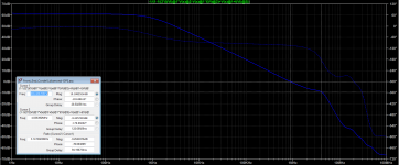
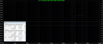
Attached is the loopgain plot with the DBT OPS. I guess that with the folded driver, this would not look much different.
There are many loopgain plots in simulation that indicate stability, but only a fraction of configurations is somewhat stable in reality.
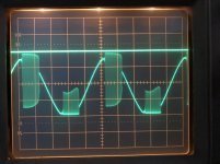
Testing for stability, I attached capacitors at the output prior to the inductor.
Square wave shows a little overshoot typical for TPC.
Note that I have the low pass filter caps at the input installed.
Adding caps at the output shows no effect on overshoot until:
At 6n8, suddenly there is some sustained oscillation on top of the square waves.
I had expected that slightly lower values show some damped ringing already.
And somehow I expected to see that the amp tolerates more capacitive disturbance.
I would guess that the stability margin is not large.
Note my squares are only +/-3V at the output.
I managed to get the amp pretty stable with the folded driver!
All it took to get there was to change the compensation: C84 is 470p and C85 is 100pF now.
The schematic I posted shows how not to do TPC, namely the caps are in the wrong location.
The large cap needs to be towards the input and the small one towards the output (of the VAS).
Probably you know this already and I'm boring you. However, I pick up such things while reading here and find it useful.
P0 is set to 470 Ohm and P4 surprised me to provide most stability at 1k5, which shapes the TPC slope pretty aggressively.
Attached is the loopgain plot with the DBT OPS. I guess that with the folded driver, this would not look much different.
There are many loopgain plots in simulation that indicate stability, but only a fraction of configurations is somewhat stable in reality.
Testing for stability, I attached capacitors at the output prior to the inductor.
Square wave shows a little overshoot typical for TPC.
Note that I have the low pass filter caps at the input installed.
Adding caps at the output shows no effect on overshoot until:
At 6n8, suddenly there is some sustained oscillation on top of the square waves.
I had expected that slightly lower values show some damped ringing already.
And somehow I expected to see that the amp tolerates more capacitive disturbance.
I would guess that the stability margin is not large.
Note my squares are only +/-3V at the output.
Attachments
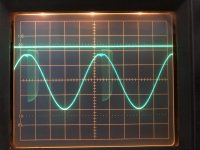
With the OPS configured as DBT, I still have the triangular oscillation.
The "old trick" to stop this by temporary tampering with the compensation still works:
Briefly connecting 100pF at C81 (MIC cap) stalls the oscillation and the amp works nicely.
Even clipping sinewaves is well behaved.
In order to revert to the unstable condition, cycling the power is enough and at next startup, the amp oscillates again.
BTW: The nice and smooth clipping is one of the main objectives for this design.
Attachments
- Home
- Amplifiers
- Solid State
- VFA front end - the Bunnyphant