Yes, a snubber of some type is an excellent way to prevent self-oscillation in many hexfets and particularly high transconductance hexfets operating at high rail voltages.
Hugh
Hugh

Hello to all VSQA designers and Builders,
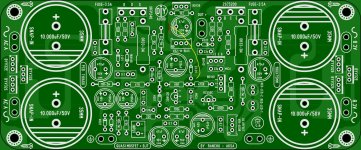
I am building the pcb's designed by Thiago. Listed below are pics of an unpopuated pcb and a semi-populated pcb and also the Schematic I am working from.


A list of the changes made to match the schematic to the pcb:
1. VR1, VR2, and KSC1845 : to match VR1 and VR2 traces to the pcb / schematic I had to mount them backwards from what is shown on the pcb. I mounted them as to what is shown on the schematic. I had to cross the base and collector of the KSC 1845 to match the pcb and schematic. I hope these where correct?
2. I am at the point where I need to follow Hugh's advice and solder one green led in place of the the 2 IN4148 diodes in series or "not". If I do use 1 green led, can I solder it into the pads for one of the IN4148 diodes and use a jumper wire in the next pads for the other 1N4148 diode, or do I have to solder additional extensions on the green led leads to stretch it across the pads for the diodes in series. This all for DC offset adjustment.
If any one has built these, or have any helpful info, I would appreciate your comments.
Thanks,
MM
I am building the pcb's designed by Thiago. Listed below are pics of an unpopuated pcb and a semi-populated pcb and also the Schematic I am working from.
A list of the changes made to match the schematic to the pcb:
1. VR1, VR2, and KSC1845 : to match VR1 and VR2 traces to the pcb / schematic I had to mount them backwards from what is shown on the pcb. I mounted them as to what is shown on the schematic. I had to cross the base and collector of the KSC 1845 to match the pcb and schematic. I hope these where correct?
2. I am at the point where I need to follow Hugh's advice and solder one green led in place of the the 2 IN4148 diodes in series or "not". If I do use 1 green led, can I solder it into the pads for one of the IN4148 diodes and use a jumper wire in the next pads for the other 1N4148 diode, or do I have to solder additional extensions on the green led leads to stretch it across the pads for the diodes in series. This all for DC offset adjustment.
If any one has built these, or have any helpful info, I would appreciate your comments.
Thanks,
MM
Thanks Eric. I will use one green led and one jumper as per the schematic. Have you built this amp?
Myles
Myles
are there big commercial available power amps on the marked with such an output stage ?The dissimilar but complementary outputs create higher evens over odds.
This leads to a pleasing sound presentation, although if some perceive higher THD the technique is bagged as an 'effects box'.
in post #9 under
New Push Pull Buffer Approach for special Kind of THD - MOSFET & BjT - New for me (schematic NAD 310 #9)
is an old simulation with schematic of such an output stage based on those from NAD 310.
P.S.: concerning this NAD model a lot of threads exist here:
NAD 310 right channel gone
NAD 310, some informs needed, Reviews, listening tests, opinions are welcome.
Nad 310 Amp
NAD 310 - need some info
NAD310 Repair
I haven’t built it yet.Thanks Eric. I will use one green led and one jumper as per the schematic. Have you built this amp?
Myles
Thanks for comments Eric and meanman1984 (Marc?). The one pic of the bare pcb above is one that I will have to throw away. I had the board almost completely soldered and one of the 1381 pads lifted off. I tried to fix the pad with solder braid, but could not get it to work. I had to desolder components and start over with a new board. Good thing that PCBway gave me an extra board in my order.
What really surprised me is the orientation of the VR1 and VR2. From the schematic's above (mine and Eric's) it clearly shows that Pin 1 (where the adjuster is) is connected to the 10K R6. Thiago's pcb has Pin 1 connecting to the diodes / leds on the Pin 3 side. Same applied to VR2, I had to look at the traces prior to mounting. I am pretty sure that I have this correct.
Eric or Marc, would you have 5 minutes spare time to check your pcb's and see if I am correct in my assessment.
Thanks for the help,
Myles
Myles ,
Don't think it matters as long pin 2 is connected at the right place . Only thing what's changes is the direction of rotation to decrease or encrease .
Don't think it matters as long pin 2 is connected at the right place . Only thing what's changes is the direction of rotation to decrease or encrease .
Thanks mm1964. I built it as described above. Getting the transistors mounted on the heatsinks, so getting closer to a power up. Will post a pic in case I have some wires wrong.
MM
MM
Hello quasi fans,
I have finished 1 channel of Thiago's Quasi pcb to the point that I could power up and set the bias and offset voltage. I am happy to say that when power was applied (using Variac slowly) that there was no smoke and the led lit up.
1. I adjusted bias voltage to 42mV across the 0.33 ohm resistors and it was stable after warm up.
2. I adjusted the DC offset voltage so that it was between -2mV and -9mV, it was moving around. I did take the bias down to around 0mV and the readings were in the +/- 5mV range.
3. The transistors on the heatsink and the heatsink itself were warm to the touch, could have left my fingers there all day.
4. The 8ohm/100W green resistor that is hooked up to the output and ground of the amp board is stone cold which I find surprising. The resistor is mounted to an solid aluminum plate approx. 3" thick, 6" wide, 8" long.
5. I think I can go ahead and hook up the inputs and speaker outs to see if music plays, but I would like some comments or suggestions from more experienced builders than me. Please see the attached pic of my setup. Thank you for your help.
Myles,
It looks pretty good, and offset -7 to -2 mV is just fine as well.
42mV bias gives you good quiescent and that's fine too.
the 8R load won't warm up until you connect a good audio source; a CD, a phone, or a siggen.
Try 1KHz 1Vpk. That should warm up your 8R load!
Cheers,
Hugh
It looks pretty good, and offset -7 to -2 mV is just fine as well.
42mV bias gives you good quiescent and that's fine too.
the 8R load won't warm up until you connect a good audio source; a CD, a phone, or a siggen.
Try 1KHz 1Vpk. That should warm up your 8R load!
Cheers,
Hugh
Thanks Hugh,
Plans are to use my laptop as the audio source. I used my laptop on the first quasi I built using the DacZ pcb. Should work OK as a test source.
Hugh, any problems in having offset cover the + and - range (ie: +/- 5mV), rather than it being only in the negative or positive range ?
MM
Plans are to use my laptop as the audio source. I used my laptop on the first quasi I built using the DacZ pcb. Should work OK as a test source.
Hugh, any problems in having offset cover the + and - range (ie: +/- 5mV), rather than it being only in the negative or positive range ?
MM
Last edited:
Patrick, I have not done that mod yet. I read about it, read Hugh's comments on it, and since there was no comments on whether it was absolutely needed or not, I left it out for now. It looks like an easy fix if needed, just have to undo the transistors and pcb to solder on the bottom of pcb.
Is there a consensus on whether it should be installed ?
Is there a consensus on whether it should be installed ?
Patrick, Hugh, Max, other builders,
Just a bit confused about the mod above.
Discussion starts on page #54- post #1062 by member spind and continues to post #1074. Post's #1068 and #1073 by Hugh are very interesting. After reading all this I am not sure that it will make a " hearable difference". Maybe a measurable difference, but I don't have the equipment or knowledge to check for that.
If soldering a wire from the C7 neg to anode of the 3v3 zener mod is necessary I will do it. I assume that no traces have to be cut on Thiago's pcb ?
Please note that Thiago had his amp playing without this mod and was experiencing no problems. His last post quoted " that he would try the C7 to 3v3 zener mod and report back". I am not aware that Thiago ever reported back, and has not been active on the forum since.
Let me know your views on this and thank you for all the help so far. Just trying to get it right 🤔
Myles
- Home
- Amplifiers
- Solid State
- Very simple quasi complimentary MOSFET amplifier