Yes, a snubber of some type is an excellent way to prevent self-oscillation in many hexfets and particularly high transconductance hexfets operating at high rail voltages.
Hugh
Hugh
Hello to all VSQA designers and Builders,
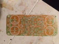
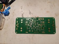
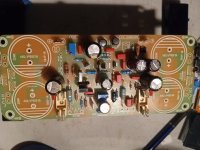
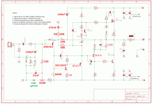
I am building the pcb's designed by Thiago. Listed below are pics of an unpopuated pcb and a semi-populated pcb and also the Schematic I am working from.
A list of the changes made to match the schematic to the pcb:
1. VR1, VR2, and KSC1845 : to match VR1 and VR2 traces to the pcb / schematic I had to mount them backwards from what is shown on the pcb. I mounted them as to what is shown on the schematic. I had to cross the base and collector of the KSC 1845 to match the pcb and schematic. I hope these where correct?
2. I am at the point where I need to follow Hugh's advice and solder one green led in place of the the 2 IN4148 diodes in series or "not". If I do use 1 green led, can I solder it into the pads for one of the IN4148 diodes and use a jumper wire in the next pads for the other 1N4148 diode, or do I have to solder additional extensions on the green led leads to stretch it across the pads for the diodes in series. This all for DC offset adjustment.
If any one has built these, or have any helpful info, I would appreciate your comments.
Thanks,
MM
I am building the pcb's designed by Thiago. Listed below are pics of an unpopuated pcb and a semi-populated pcb and also the Schematic I am working from.


A list of the changes made to match the schematic to the pcb:
1. VR1, VR2, and KSC1845 : to match VR1 and VR2 traces to the pcb / schematic I had to mount them backwards from what is shown on the pcb. I mounted them as to what is shown on the schematic. I had to cross the base and collector of the KSC 1845 to match the pcb and schematic. I hope these where correct?
2. I am at the point where I need to follow Hugh's advice and solder one green led in place of the the 2 IN4148 diodes in series or "not". If I do use 1 green led, can I solder it into the pads for one of the IN4148 diodes and use a jumper wire in the next pads for the other 1N4148 diode, or do I have to solder additional extensions on the green led leads to stretch it across the pads for the diodes in series. This all for DC offset adjustment.
If any one has built these, or have any helpful info, I would appreciate your comments.
Thanks,
MM
Thanks Eric. I will use one green led and one jumper as per the schematic. Have you built this amp?
Myles
Myles
are there big commercial available power amps on the marked with such an output stage ?The dissimilar but complementary outputs create higher evens over odds.
This leads to a pleasing sound presentation, although if some perceive higher THD the technique is bagged as an 'effects box'.
in post #9 under
New Push Pull Buffer Approach for special Kind of THD - MOSFET & BjT - New for me (schematic NAD 310 #9)
is an old simulation with schematic of such an output stage based on those from NAD 310.
P.S.: concerning this NAD model a lot of threads exist here:
NAD 310 right channel gone
NAD 310, some informs needed, Reviews, listening tests, opinions are welcome.
Nad 310 Amp
NAD 310 - need some info
NAD310 Repair
I haven’t built it yet.Thanks Eric. I will use one green led and one jumper as per the schematic. Have you built this amp?
Myles
Thanks for comments Eric and meanman1984 (Marc?). The one pic of the bare pcb above is one that I will have to throw away. I had the board almost completely soldered and one of the 1381 pads lifted off. I tried to fix the pad with solder braid, but could not get it to work. I had to desolder components and start over with a new board. Good thing that PCBway gave me an extra board in my order.
What really surprised me is the orientation of the VR1 and VR2. From the schematic's above (mine and Eric's) it clearly shows that Pin 1 (where the adjuster is) is connected to the 10K R6. Thiago's pcb has Pin 1 connecting to the diodes / leds on the Pin 3 side. Same applied to VR2, I had to look at the traces prior to mounting. I am pretty sure that I have this correct.
Eric or Marc, would you have 5 minutes spare time to check your pcb's and see if I am correct in my assessment.
Thanks for the help,
Myles
- Home
- Amplifiers
- Solid State
- Very simple quasi complimentary MOSFET amplifier