Good idea Eric, I'd been using my cell phone and it does not have the flexibility to drop in the schematic when mid-sentence....... good call.
Terry, and confirmed by XRK, to achieve -1.471V at the wiper you replace the two redleds #1 and #2, and wire in two 1N4148s. This will deliver you just over -1.3V to pin 3 of VR1. The other side of VR1 is connected to the negative rail VIA R6, 10k. With a -35V rail, you will then have a range at the wiper from -1V32 to -1V96. This is right in the 1.71V zone, and you can set the output (warm) at 0mV offset.
The bias generator, that is the Vbe multiplier Q4 and zener/led D7) will run at (35-4.2)/(2k2+1k2) = 9mA stable. Therefore the current through the 3.3V zener (or blue led, or greenled+4148) will also be 9mA. For most blue leds this is very, very bright and will burn a hole in your head, however a greenled passes this current comfortably and looks pretty special.
Hope this is clear as mud! the simple idea is to get offset to less than +/-10mV and adjust the quiescent to around 100mA.
Hugh
Hi Hugh,
Of course I am still trying to learn these things. By changing from two LED to two 1N4148, are we raising the bias on Q1?
Of course I am still trying to learn these things. By changing from two LED to two 1N4148, are we raising the bias on Q1?
Well, I tried putting two 1N4148s in place of the two red LEDs and it didn't like that at all. Offset was very high. So I paralleled a 100k trimmer with the 51k R5 so I could adjust it. By adjusting the two trimmers I was able to get close to 0 offset but it was all over the place, constantly moving in about a 30mV range. I couldn't get it to settle at all. I pulled the diodes and replaced the two red LEDs and it is playing perfectly. I think I will leave well enough alone.
..... replace blue LED with a green plus 1n4148 for a more subdued light. But if you are good with blue light I wouldn't change it.
Why not just use the preferred LED and put a black heat shrink tube over it ? It will block the 'unwanted' bright light ! You will get just a bit leaking from gaps from the underside of the LED. The top can be plugged with something while heat shrinking the small tube !
The voltage reference at the two redled/4148 on the input base of Q1 is dependent on FOUR inter-related factors, and all must align to permit offset adjustment to 0mV. Trace these issues through the schematic (quasi-rev2 from Prasi as annotated by Thimios).
1. The current through Q1 which is set by R7 between base and emitter of Q2.
1K sets a collector current in Q1 of 0.62mA. If you change R7 the potential needed at base of Q1 must change.
2. The bias resistor to base of Q1, I choose 33k but if you change this up to 150k you will RAISE the offset voltage at output. I choose 33k to keep the offset from wandering, as Terry has found.
3. The value of R9, the 1K feedback resistor. If you increase this, the offset will RISE for the same voltage reference at LED1 and 2.
4. The beta (hfe) of Q2. Higher beta will LOWER the offset.
Now, to tie this down at offset 0mV, we have to choose these resistors.
I suggest R5 at 33k. This dominates the Zin of the amplifier. Anything higher than this and the offset control starts to wander.
I suggest we leave R7 AND R9 BOTH STAY AT 1k.
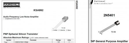
Lastly, I suggest 2N5401 for Q1. This will have a beta around 100, leading to a base current of 7uA. 7uA will drop 0.23V across R5, so whatever is at the wiper of the offset trimmer will be HIGHER by 0.23V.
Since the voltage at the output has to be at 0mV, then the voltage drop across R9 (fb resistor which flows 0.62mA) plus the Vbe of Q1 (o.62V) plus the dropped voltage across R5 (0.231V) will give use the voltage we need at the wiper of trimmer VR1. This comes to -1.471V needed at the wiper.
You CANNOT deliver -1.471 at the wiper of VR1 is you have two redleds at LED1 and LED2. The highest voltage you will deliver is no higher than -3.2V, and it might actualy be higher, maybe -3.50V. This is TOO LOW, so if R9 and R7 are 1K and R5 is 33k, you will have an offset of -2V, way off!
SOLUTION:
Set R9 to 1k 1W
Set R7 to 1k
Set R5 at 33k.
R&R the redleds for two 1N4148s in series.
Leave R6 at 10k 1W.
This will give you an offset of 0mV +/-10mV when you set the trimmer VR1.
Cheers,
Hugh
1. The current through Q1 which is set by R7 between base and emitter of Q2.
1K sets a collector current in Q1 of 0.62mA. If you change R7 the potential needed at base of Q1 must change.
2. The bias resistor to base of Q1, I choose 33k but if you change this up to 150k you will RAISE the offset voltage at output. I choose 33k to keep the offset from wandering, as Terry has found.
3. The value of R9, the 1K feedback resistor. If you increase this, the offset will RISE for the same voltage reference at LED1 and 2.
4. The beta (hfe) of Q2. Higher beta will LOWER the offset.
Now, to tie this down at offset 0mV, we have to choose these resistors.
I suggest R5 at 33k. This dominates the Zin of the amplifier. Anything higher than this and the offset control starts to wander.
I suggest we leave R7 AND R9 BOTH STAY AT 1k.
Lastly, I suggest 2N5401 for Q1. This will have a beta around 100, leading to a base current of 7uA. 7uA will drop 0.23V across R5, so whatever is at the wiper of the offset trimmer will be HIGHER by 0.23V.
Since the voltage at the output has to be at 0mV, then the voltage drop across R9 (fb resistor which flows 0.62mA) plus the Vbe of Q1 (o.62V) plus the dropped voltage across R5 (0.231V) will give use the voltage we need at the wiper of trimmer VR1. This comes to -1.471V needed at the wiper.
You CANNOT deliver -1.471 at the wiper of VR1 is you have two redleds at LED1 and LED2. The highest voltage you will deliver is no higher than -3.2V, and it might actualy be higher, maybe -3.50V. This is TOO LOW, so if R9 and R7 are 1K and R5 is 33k, you will have an offset of -2V, way off!
SOLUTION:
Set R9 to 1k 1W
Set R7 to 1k
Set R5 at 33k.
R&R the redleds for two 1N4148s in series.
Leave R6 at 10k 1W.
This will give you an offset of 0mV +/-10mV when you set the trimmer VR1.
Cheers,
Hugh
Last edited:
I'm glad I took a much needed nap. Now more definitive steps are presented. Should I go ahead and swap Q1 with 2n5401 in addition to the R9=R7=1k, R5=33k, R6=10k 1W, 1n4148 x2 for LEDs ?
Warning the iron now and making some coffee. 🙂
Warning the iron now and making some coffee. 🙂
Quasi Success!
Well, I spent nearly two hours trying to fix the amp that I fried and also implementing upgrades with no success. It still pegs the current on the 10R safety resistor at 17v or 1.7amps when turned on. I even replaced the IRFP240 and same result. I guess I have to go in and replace all transistors one by one or could it be something like a burned out pot or blown diode etc.? What a waste of time that was. Basically put it aside to get the frustration down.
I then went on to my other channel which was never tested with a good audio source and just went ahead and replaced the R9 and R7 with 1k. I had to make a 1w 1k resistor by series-parallel qnty 4 x 1k 0.25w resistors. I installed two 1n4148's in place of the red LED's. Put black shrink tubing over the obnoxious blue LED. Plugged it in and fired here up. Bias was stable and adjusted to 22mV across 0.22R for 100mA quiescent current. Now the money shot: is the DC offset good? Drum roll.... well yes, almost. I can now get -23mV DC offset. It responds to the offset pot but that is just the limit. I am running 500R pot, so what can I do to get it to 0mV? Can I change the 33k R5 to another value? Or add a resistor in parallel to the pot to get the value lower? Would switching to 2n5401 help to fix the DC offset issue even further?
I am listening to music now. Sounds great! The bass is very nice. The over all sound is very pleasing, sweet and delicate. I can do an A/B test with the JK VSSA on the left speaker and the quasi on the right.
It's holding it's own.
Hugh, thanks for all your help in getting this to work! Could not have done it without you.
Do you have any suggestions on how to go about fixing my fried amp? I think you said check Vbe of each BJT and it needs to be 0.55v to 0.65v?
Edit: Q3 and Q5 are running relatively cool now - not hot at all. So the changes seems to have helped in this respect too. No heatsink needed.
So, in summary here are the changes needed for this amp to work - use Hugh's recommendations:
SOLUTION:
Set R9 to 1k 1W
Set R7 to 1k
Set R5 at 33k.
R&R the red LEDs for two 1N4148's in series.
Attachments

Last edited:
take out the safety resistors in the power rails.
Power ON via a Mains Bulb Tester. The bulb will probably glow bright.
That reduces the voltage fed to the transformer and your supply rails will probably be less than ±5Vdc.
You can probe around the PCB to see if any of the transistors are being fed with some Vbe and measure that. Might give you a clue.
XRK , did your short the input?
Yes, actually a 10R resistor between the inputs was used for purposes of checking DC offset.
Hi XRK,
Good work. Slowly you recover your confidence. This is crucial. When you get there you will have known the misery, and it's only from the depths of despair that you can appreciate the wonder of a really good amp. Trust me, I've been here many times.....
Now, add a 220R between the left side of VR1 and the second 4148. Can you do some measuring now?
What is the voltage wrt ground (black probe!) on the:
1. OUTPUT (I assume at present -23mV is your total end of the range?)
2. Base of Q1.
3. Wiper of VR1, and pin 3, near the 4148.
This should nail it for the good module. Then we look at the #1 hombre....... and don't change the 33k R5, it will mess with the offset stability.
Hugh
Last edited:
why the 10R resistor I always do without
To provide a convenient handle for me to pull off the 0.10in pitch two terminal header connector. They are tiny and in a slightly inaccessible location. 🙂
@Aksa: unfortunately, I have to head off to work (the paying kind) and revisit this when I get back tonight. I will measure base of Q1. The output is at end of range and is -23mV.
I hope the 220R will get me the room I need to adjust the offset to zero.
Haha, LOL, the depths of despair in amp building. Yes, pretty much about where I was. 😱
The balance point in this amp seems a bit tricky. Would much of this have been caught in simulation - we did run a sim didn't we before committing to PCB layout? I can't remember now. It would be good to go in and update sim with these latest values and see what we get. For some reason, seems people have blue LEDs but not a 3.2v Zener. With removal of two red LEDs having that blue one is good (if covered with black shrink tubing).
Last edited:
XRK,
I hope that at work you pull off six successes in the space of six hours........
Then you will be cocky to take on #2 monster!
Yes, simulation will give you very precise operating points. If you have good models, and many are very ordinary.
Hugh
I hope that at work you pull off six successes in the space of six hours........
Then you will be cocky to take on #2 monster!
Yes, simulation will give you very precise operating points. If you have good models, and many are very ordinary.
Hugh
Thanks Hugh. I'm going to need that 6 for 6 good luck at work. Dealing with some big problems in real life work. 🙂
- Home
- Amplifiers
- Solid State
- Very simple quasi complimentary MOSFET amplifier