To find what's happening on the circuit, could you please measure these areas:
1. Voltage across Vbe multiplier, Q4, from C to E of BD139. Should be 1.90 volts
2. Voltage across LED and series 4004 diodes. Should be 3.25 volts
3. Voltage from gate of Q6 nmos to base of inverter, Q5. Should be 5.19 volts.
4. Voltage across R20, for 0.47R this should be around 50mV
5. Voltage at output wrt ground, should be 0mV but I think it's about +2? (positive?)
6. Voltage wrt ground at left side of VR1, should be -3.2V.
7. Voltage wrt ground at right side of VR1, should be -3.82V.
8. Voltage at wiper of VR1, and voltage at base of Q1, all wrt ground.
A lot of these pins/points are not exposed on the topside of the amp. I will have to flip amp upside down but then there is no heatsink. I am flipping amp to side and getting back pins where possible.
1. 2.13v for 400mA current.
2. voltage across 2 red LEDs is 3.50v
3. nmos G (-) tp Q5 base (+) is -5.06v
4. R20 voltage is 90mV across 0.22R (I adjusted this for 400mA current).
Normally I run 80mA but trying to see if XO distortion goes away - no.
5. -1.3v is lowest I can get it
6. -4.76v (I think this is what you are calling the "right" side of the vr1)
7. -3.50v (side facing top edge where Fastons are)
8. voltage at wiper of VR1 is -3.50v
Thanks.
X
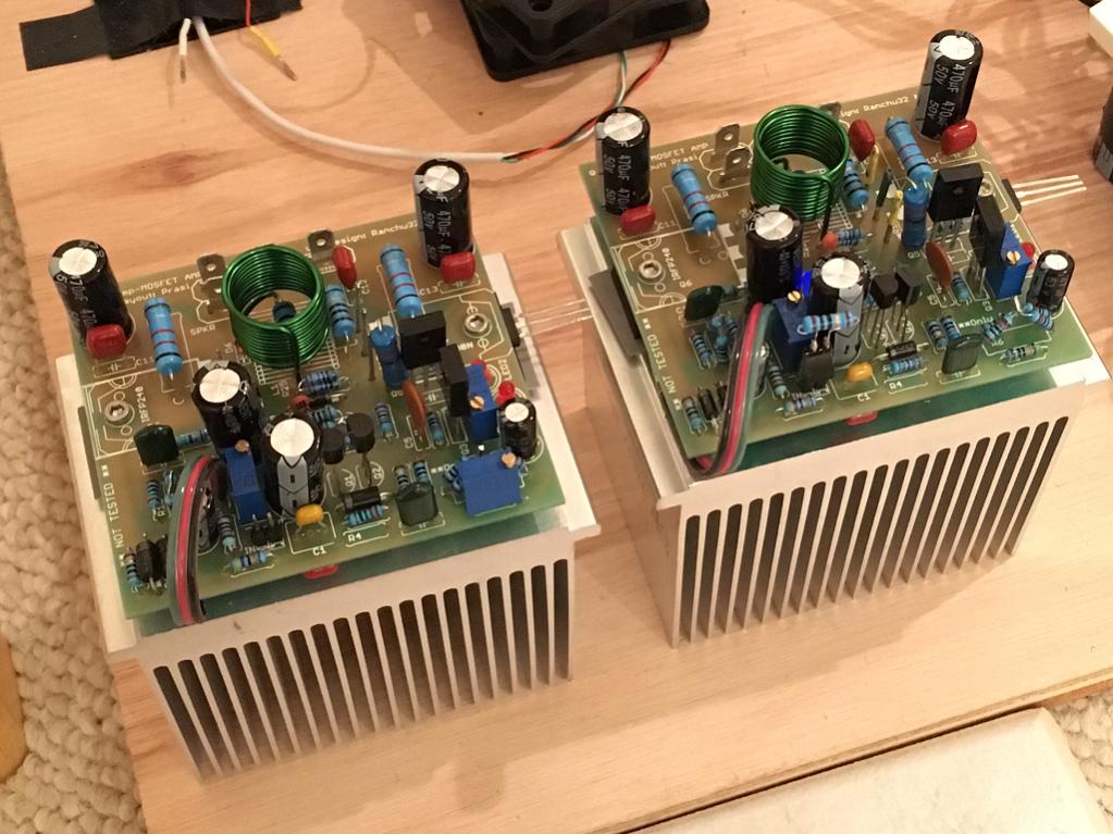
It's too bad I am having so many problems because it's a cute looking little amp as it fits these Dell Pentium CPU heatsinks perfectly.:
Attachments

Last edited:
Hi XRK,
We are getting very close to fixing this.........
This will identify this..........
Hugh
We are getting very close to fixing this.........
To find what's happening on the circuit, could you please measure these areas:
1. Voltage across Vbe multiplier, Q4, from C to E of BD139. Should be 1.90 volts
2. Voltage across LED and series 4004 diodes. Should be 3.25 volts
3. Voltage from gate of Q6 nmos to base of inverter, Q5. Should be 5.19 volts.
4. Voltage across R20, for 0.47R this should be around 50mV
5. Voltage at output wrt ground, should be 0mV but I think it's about +2? (positive?)
6. Voltage wrt ground at left side of VR1, should be -3.2V.
7. Voltage wrt ground at right side of VR1, should be -3.82V.
8. Voltage at wiper of VR1, and voltage at base of Q1, all wrt ground.
A lot of these pins/points are not exposed on the topside of the amp. I will have to flip amp upside down but then there is no heatsink. I am flipping amp to side and getting back pins where possible.
1. 2.13v for 400mA current.
2. voltage across 2 red LEDs is 3.50v
HD: This gives us a total bias voltage of 2.13+ 3.50= 5.63. This is a heavy bias; you could increase the resistance in the BASE to EMITTER of the Vbe multiplier so that the voltage across the entire shebang reduces to Thimios' value, that is 5.19V rather than 5.63V. This should reduce the idle current around 100mA, and if it's 400mA it should be then 300mA, but to be honest this is a bit too high. I would not use more than 150mA. Even then it will be pretty warm, this is 0.15 x 70 = 10.5W, about what it should have.
3. nmos G (-) tp Q5 base (+) is -5.06v
HD: This confuses me. What is the voltage from GATE of nmos Q6 to BASE Q5 pnp? It should be 5.20V, no more.
4. R20 voltage is 90mV across 0.22R (I adjusted this for 400mA current).
Normally I run 80mA but trying to see if XO distortion goes away - no.
HD: 90mV across 0.22R is 410mA and you will be dissipating around 28.7W across your heatsink for each channel. This is far too high and you need to reduce your bias generation by increasing Vbe resistance on the Vbe multiplier as above.
5. -1.3v is lowest I can get it
HD: You need to put the black probe on the ground, negative probe is always on GROUND, and red probe on the output. If you do this should get +1.3, not negative, and the next question is this: CAN YOU GET THIS VOLTAGE UP CLOSE TO ZERO?
6. -4.76v
7. -3.50v (side facing top edge where Fastons are)
HD: This is wrong way around. I should read -3.5V (black on grnd, red on left side of VR1 near leds) and -4.76V wrt ground on the RIGHT side of the VR1, near 10k 1W R6. Is this correct?
8. voltage at wioer of VR1 is -3.50v
HD: Have your removed R4, and replaced R5 with 33k? What is the voltage, with black on gnd and red on base of Q1, wrt ground now?
This will identify this..........
Hugh
Last edited:
Couldn't sleep so I hooked it up and measured. Rails +-36.3VHi XRK,
I gotta get into this and try to help. I'm sorry you are in trouble, but it will be very simple once we find it. Measurement is the best way.
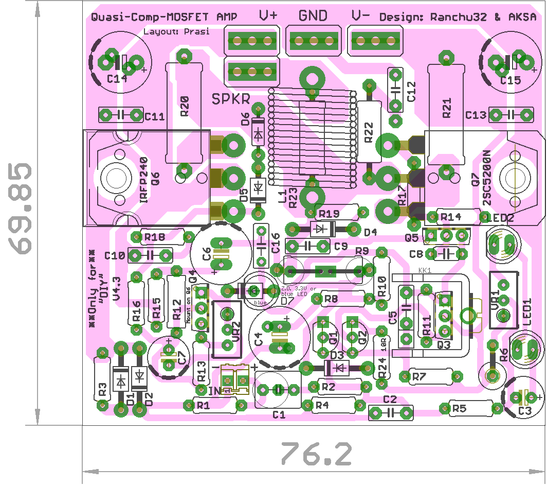
Now, index our circuit. You are working from Prasi's Rev 4.3 here?
http://www.diyaudio.com/forums/solid-state/255427-very-simple-quasi-complimentary-mosfet-amplifier-68.html
This is #675.
To find what's happening on the circuit, could you please measure these areas:
1. Voltage across Vbe multiplier, Q4, from C to E of BD139. Should be 1.90 volts 2.051V
2. Voltage across LED and series 4004 diodes. Should be 3.25 volts 3.665V
3. Voltage from gate of Q6 nmos to base of inverter, Q5. Should be 5.19 5.09Vvolts.
4. Voltage across R20, for 0.47R this should be around 50mV (0R33) 38mV
5. Voltage at output wrt ground, should be 0mV but I think it's about +2? (positive?) 0.5mV
6. Voltage wrt ground at left side of VR1, should be -3.2V. -3.667V
7. Voltage wrt ground at right side of VR1, should be -3.82V. -4.33V
8. Voltage at wiper of VR1, and voltage at base of Q1, all wrt ground. -3.98 / -1.835V
That should be enough to identify all currents and voltages around this circuit.
Good luck!
Hugh
You can see my findings above in red.
Post #483 is the schematic as built with measurements
That is why i post schematic and measurements always,easy debugging.
Last edited:
Thanks for all the help guys. Sorry to leave you hanging but had to stop last night at 3am. Will investigate again later today following your tips and questions to debug.
I am just realizing that I may be the first to make this amp with this particular layout. This layout is different than what Terry made from his own etching? I wonder if there is an issue with the circuit and layout as implemented here as I have same problem on both boards. So if it's a user error like cold solder joint or bad trace - odds of same error on both is low.
So, if I am the first on this particular layout - I can recalibrate my expectations and not feel as frustrated as it would be indeed sort of like "path finder" mode.
Luckily, in the past on Prasi's layout - they all fired up and ran from the get go. This one is a special animal - clearly off the beaten tracks and should be given more consideration accordingly.
Thanks for all your patience and help though. I would indeed be at a dead end without your expertise.
It appears that I'm late to the party this time.
If you can mark up, scan and upload, a printed version of the schematic your working to with voltages at each of the nodes, I'm certain one of us can help get to the bottom of this in no time.
If you can mark up, scan and upload, a printed version of the schematic your working to with voltages at each of the nodes, I'm certain one of us can help get to the bottom of this in no time.
To minimize the possibility,where you get the pcb?
From bangla H
I've the same boards can't test them myself missing some parts
I got my boards from BanglaH - not sure which board house made them. They look to be pretty good quality compared to other boards I Have had made.
I know but I've the same boards.
xrk did measured 90mV across R20(0R22 in xrk case) isn't that way to much?
xrk did measured 90mV across R20(0R22 in xrk case) isn't that way to much?
I know but I've the same boards.
xrk did measured 90mV across R20 isn't that way to much?
That was just me pushing bias current high to see if distorted sound could be improved. I normally would run at 80mA across 0.22R for 18mV. I will set it back to 18mV for next round of tests.
I can be wrong but I think the bias setting and offset settings are some kind related to eachother.
That was just me pushing bias current high to see if distorted sound could be improved. I normally would run at 80mA across 0.22R for 18mV. I will set it back to 18mV for next round of tests.
Meanman did ask this, is Q4 wired correctly? I have a guess that its connected wrongly
reg
prasi
It's connected according to the layout with proper orientation of pin 1 where square pad is. If it was backwards I would not be able to effect bias current adjustment at all. I just noted on the layout diagram that blue LED orientation is incorrect as drawn. It would be opposite of a Zener as they work in reverse polarity breakdown voltage. I can confirm that amp hits the rails if LED is in backwards.
Note that this is not the board I have as mine says not tested and has no provision for heatsink on Q3/5
Note that this is not the board I have as mine says not tested and has no provision for heatsink on Q3/5
Last edited:
Thanks for all the help guys. Sorry to leave you hanging but had to stop last night at 3am. Will investigate again later today following your tips and questions to debug.
I am just realizing that I may be the first to make this amp with this particular layout. This layout is different than what Terry made from his own etching? I wonder if there is an issue with the circuit and layout as implemented here as I have same problem on both boards. So if it's a user error like cold solder joint or bad trace - odds of same error on both is low.
So, if I am the first on this particular layout - I can recalibrate my expectations and not feel as frustrated as it would be indeed sort of like "path finder" mode.
Luckily, in the past on Prasi's layout - they all fired up and ran from the get go. This one is a special animal - clearly off the beaten tracks and should be given more consideration accordingly.
Thanks for all your patience and help though. I would indeed be at a dead end without your expertise.
Hi X,
Terry used the layout from post #333 http://www.diyaudio.com/forums/soli...imentary-mosfet-amplifier-34.html#post4765108 .
Bangle H ordered the PCB from the same post. So PCB layout works, so there should be a problem with build unless its a manufacturing issue, which I doubt very much.
reg
Prasi
Last edited:
- Home
- Amplifiers
- Solid State
- Very simple quasi complimentary MOSFET amplifier