Valery nailed it. Raise on end of R10 and the amp will be operating entirely in global feedback, with minimal THD. Connect up R10 and the global feedback will be reduced to 68/1.8 = 37.8 = 31.54dB. This obviously increased the THD, BUT, it does change the profile of the THD, increasing the H2-H5, and there is another effect you might find that most people would not notice at all.
BTW, to be fair, 'intuitive' logic is as often incorrect, so it's very careful to be absolutely sure of this. I explain the words nicely; the concept might not be so wonderful! A lot of dubious concepts are beautifully described with 'perceived' logic.......
This is quite interesting and I can even make measurements at the speaker and sound clips to share to see if anyone hears a difference. Level adjusted for same SPL of course.
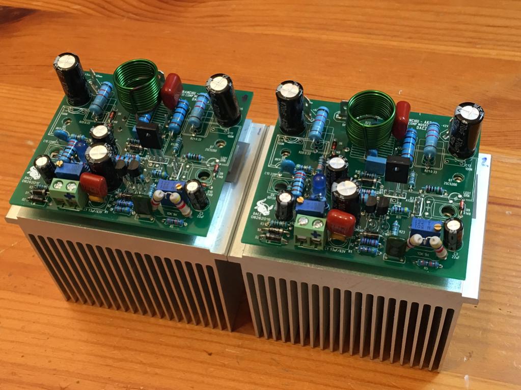
The Dacz boards are both completed and tested. Setup was smooth and easy on both. An excellent board that is easy to build. At 100mA bias (35v rails), I do not need a fan for the little Pentium heatsink that I am using. Very compact hifi setup. Sounds fantastic - long term listening and some speaker measurements next and I will report back with overall impressions. I am using higher quality components so I expect the sound should be better - but you never know. These are also the Onsemi NJW0281G NPN outputs. Seems to be working very well though.
Absolutely a frustration free build and startup. The bugs on this can be definitively said to be "all worked out". Anyone should be able to take these Gerbers and BOM and have a good time now. 🙂
Here is a list of the substitutions that I used on this build of the Dacz board, so that it is clear where I deviated from the BOM.
All resistors metal thin film 1% 1/4W unless otherwise specified
R5 = 27k
R6 = 2 x 4k7 carbon 1W 5% in series
R8 = 100R
R9 = 2k2 (gain is defined by R9 & R8, and is a bit lower in my case)
R12 = 2k2 1W
R13 = 1k + 220R in series
R15 = 2 x 3k3 in parallel
R17 = 10R
R19 = 100R
R20 & R21 = 0.22R 2W
C1 = 10uF 50V X7R & 1uF 250V Film in parallel
C3 = 47uF 63V
C4 = 1000uF 25V
C5 = 22pF 50V NP0/C0G SMT
C10 = 330pF 1000V ceramic
C11 & C13 = 100nF 50V X7R SMT
C12 = 100nF 250V Film
LED1 = not used
LED2 = Blue LED
D7 = not used
Q6 = Vishay IRFP240
Q7 = Onsemi NJW0281G
It might be worth trying an mkp 220pF 100V for C10.
A high K ceramic for C10 will change capacitance as the voltage swings, especially when it swings very high.
A high K ceramic for C10 will change capacitance as the voltage swings, especially when it swings very high.
I have some 220pF 100v film caps on order. Can't believe I ran out of those unexpectedly.
This amp so far measures slightly better than previous quasi from distortion at speaker as measured with microphone. Bass performance is slightly cleaner. So far very nice sounding - no complaints.
The nice thing about a compact 50w amp like this is possibility of doing a "lobotomy" on an existing commercial amp in a case. Just pull out existing discrete power amp board and replace with something small like this. My Yamaha RX360 is a good candidate. Of course, stock PSU probably is not up to the task compared to a 250VA toroidal and nice CRCLC filter. Also, this is such a pretty amp - be a shame to cover it up 🙂
Last edited:
Hello everyone.
I need a little clarification.
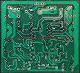
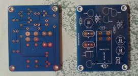
In the photo of pcb DACZ, framed in red is a double track?
I'm made of double-sided pcb double for two runs, same thing?
Thank you.
No, it's a single track with green solder mask applied and left middle of track exposed.
thank you for that clarification! 🙂No, it's a single track with green solder mask applied and left middle of track exposed.
does anyone know why he left the solder mask off some of the traces?No, it's a single track with green solder mask applied and left middle of track exposed.
What purpose does that serve?
does anyone know why he left the solder mask off some of the traces?
What purpose does that serve?
To add additional copper wire ? 😀
To add additional copper wire ? 😀
to both I ask:Usually add solder.
what purpose does that serve?
to both I ask:
what purpose does that serve?
I have to agree with Andrew here. If the copper trace is wide and/or thick enough to carry the needed current, adding solder on top does not help at all since lead or tin is a far worst conductor than copper. Better have the proper trace in the first place.
Do
Not paying the extra thickness to the boardhouse, and still having augmented thickness trace where You feel it is needed?
I guess you could always solder a copper wire on top but I don't know how good this would be in the end. I checked and making those PCBs in 2oz copper is about 3.50$ /PCB which ain't bad at all but if 1oz copper is sufficient because the traces width make up for it then it is money wasted. Unfortunately not too many of us can really measure this, at least not me. And maybe at low to moderate sound levels it is a no brainer anyways.
Do
Last edited:
Since there is already a 0.33R source/collector resistor in place, I doubt you need thicker traces to reduce the ohmic drop across that 1in travel of copper trace. The resistive drop there is much smaller than 0.33R.
2oz copper PCBs (under 100mm Sq) cost substantially more (more than 2x) than 1oz. If you are building for home use and fun and trying to keep costs down - doesn't make sense. If you expect a lot of reworking, it makes repairs easier from standpoint of durability from pad peel off. But with good design making pads bigger around parts that need exchangingos often enough. Transistors for example should have bigger oversized pads.
2oz copper PCBs (under 100mm Sq) cost substantially more (more than 2x) than 1oz. If you are building for home use and fun and trying to keep costs down - doesn't make sense. If you expect a lot of reworking, it makes repairs easier from standpoint of durability from pad peel off. But with good design making pads bigger around parts that need exchangingos often enough. Transistors for example should have bigger oversized pads.
Last edited:
XRK,Since there is already a 0.33R source/collector resistor in place, I doubt you need thicker traces to reduce the ohmic drop across that 1in travel of copper trace. The resistive drop there is much smaller than 0.33R.
2oz copper PCBs (under 100mm Sq) cost substantially more (more than 2x) than 1oz. If you are building for home use and fun and trying to keep costs down - doesn't make sense. If you expect a lot of reworking, it makes repairs easier from standpoint of durability from pad peel off. But with good design making pads bigger around parts that need exchangingos often enough. Transistors for example should have bigger oversized pads.
do you have any idea what purpose the missing solder resist serves?
I did not design the layout but have seen numerous times, Destroyer X (Carlos), goop on (add many layers) maybe 3mm thick extra solder on the traces - I assume to increase current capability? It comes in handy when you solder the large parts as the solder trace really heats up due to thermal conductivity of a large trace and I fear the resist would just thermally degrade and burn up. Hence better to leave off so it doesn't look like a charred mess.
Why don't we just ask Dacz? I have seen this done on Sonal's layouts as well.
Why don't we just ask Dacz? I have seen this done on Sonal's layouts as well.
Last edited:
interesting topic. my question would be what harm does it (leaving the solder mask off) do for the power and spk out traces?
No I think but it's less beautiful! 😀interesting topic. my question would be what harm does it (leaving the solder mask off) do for the power and spk out traces?
I don't think it does a lot of good where prolonged high current is expected as the solder will begin to melt, but certainly for protection against a surge it has some merit. It does no harm. From one who does mostly home etched boards, I don't find it unsightly. 😀
- Home
- Amplifiers
- Solid State
- Very simple quasi complimentary MOSFET amplifier