Bonjour Hugh,
Yes, it is my design, but as I wrote on the previous post I took several ideas from people publishing amplifier on the forum and from book like the very good one from Merlin Blencowe : Designing High-Fidelity Tube Preamps ( Designing High-Fidelity Valve Preamps by Merlin Blencowe (Hardcover) - Lulu )...
For the speaker DC protection, I took the schema of Project16 that was used in the Quasi and for the MOSFET output, I have been inspired by an old hybrid design found on the Web : The but as you can see I have changed a lot of things because I didn't want a class A output stage 🙂
Since I was not sure that all these modifications were good, your feedback help me to go ahead and to build it to see if we can merge the best of both world, tube input for second harmonic good distortion and MOSFET output for good current drive 😀
In fact I discovered the interest of MOSFET after reading Merlin book and the thread from Ian (gingertube) about the EL84 Baby Huey, and since that time I love MOSFET used in source follower instead of tube, since they are doing the job very well and much more easily (no heater at 75 V by example) 🙂
I am also planning to use them to replace cathode follower drivers in a new version of the TENA amplifier too ( The Emperor's New Amplifier )...
Cheers,
Marc
Hi Hugh,
Finally I have found from where I started this project, it was a schema published in 2003... It is no more on the web except as an archive, you can find it here : 6FQ7/6SN7 + MOS. FET Hybrid power amplifier !
As you can see I modified the SRPP with a MOSFET on the top device like I have done in a preamplifier with good result 🙂
Dis you think that it is possible to modify the connexion between the tube stage and the MOSFET output, because I don't like to have two 0.1 uF capacitors in serial ? If I understand this is used to bias the MOSFET ? Could we use a bias circuit with a BD139 by exemple ?
Cheers,
Marc
Hi Marc,
I too looked at the interface tube/mosfet and wondered why it was done.
After careful thought, I believe it was done to prevent cross conduction of the output during switch on, where this amp could threaten the output devices and even the speaker.
The two caps are carefully selected and rather low value. However, we are driving lateral fets, which have small gates with low capacitance. While I would tempted to move to 0.47uF rather than 0.1uF I suspect it would be very difficult to control the switch on pulses, and to that end it's a bit of a compromise.
Your heavy drive out of the second triode is commendable, but hugely diminished by the very low caps which lead to the important gates. You do need two caps here in series to prevent big thumps passing to the outputs. If you do increase these caps to 0.47uF each, then the 220k bias resistors will have to be reduced to 47k. This will change the dimensions of the bias string too; halve every value at least.
An option would be to drive not the output gates, but a very small complementary high voltage jfet, or even mosfet such as DN2540. Then the source of this small fet could attach to the gate with powerful drive, whilst maintaining switch on pulses. BUT, that adds complexity and with the very low drive requirement of the laterals I would expect that this would sound very, very good. It is Class A SE tube voltage amplification to a well controlled PP output stage, and it should sound superb.
Another option might be a relay which holds tube output off the mosfet input circuit until three seconds have passed. You would leave the relay OFF at switch on connecting tube output after the first cap to ground, then after three seconds pull the tube output to the output stage.
As it stands, I suspect it would beat many high quality SS amplifiers in the market. However, I suspect it would have somewhat soft bass; musical, but not hard hitting. I would build it exactly as it is, and see how it goes. It might be just perfect as it stands..... and the ear is the final judge!
Ciao,
Hugh
Last edited:
Hi Hugh,
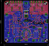
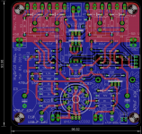
Thanks for your explanations, as you suggest I will keep the schema as it is 🙂 However, I have modified the layout a lot, after a rev. 3 were I modified capacitors pattern to accept bigger size, I finally decided to put the power MOSFET vertically to be able to build the amplifier in a low profile case with the tube mounted vertically, this is the Rev. 4 😀
This give me the opportunity to put larger capacitor and to improve a little bit the layout (don't worry for the PMOS symbol on the schematic)...
In your comment you speak about lateral fets, but I don't think that the IRFP240 & IRFP9240 are lateral MOSFET ?
For the power on thumps, I will use Project16 DC protection logic with power on delay, it will drive the on board solid state relay therefor there should be no problem 🙂
If I don't find any problem during a last check tomorrow morning I will send the files to PCBWay...
Thanks again for your help & best regards,
Marc
Attachments
Hello Marc, Hugh
I was able to set one channel exactly as per the specs with 45mV across the 0.33 resistor biasing with DC offset hovering around 0.02-0.4mV and stable. Now when I started setting up the second channel today I think my screw driver skidded on the biasing trimmer VR2 and touched some resistor or the diode close to that the trimmer, the DC offset started jumping like going all the way to 41v and the before I could even switch off the amp R14 (150R 0.24W) resistor got burned with a bit of spark/smoke. I replaced this with another 150R 0.5W one and now when I power it my CRC PSU board started heating up like the 0.33R resistor got so hot that I could see them turning to hot red 🙁 . Immediately switched off the amp. I disconnected the amp and ran the PSU alone and it was running fine with stable output of +/- 44.1Vdc, so the PSU is having issues only when the amp board is connected. Looks like something on the amp boards is drawing more current which is making the PSU CRC resistors turn very hot.
Not sure what went wrong during my stupidity. Any ideas what went wrong and where should I look for this as the other board is working fine and absolutely no issues.
thanks
Last edited:
probably you have shorted the output or some tranny on amp, which is drawing excessive current, making the resistor on the PSU heat up.
Check your amp module and the transistors for shorts.
regards
Prasi
Check your amp module and the transistors for shorts.
regards
Prasi
Hi Hugh,
Thanks for your explanations, as you suggest I will keep the schema as it is 🙂 However, I have modified the layout a lot, after a rev. 3 were I modified capacitors pattern to accept bigger size, I finally decided to put the power MOSFET vertically to be able to build the amplifier in a low profile case with the tube mounted vertically, this is the Rev. 4 😀
This give me the opportunity to put larger capacitor and to improve a little bit the layout (don't worry for the PMOS symbol on the schematic)...
In your comment you speak about lateral fets, but I don't think that the IRFP240 & IRFP9240 are lateral MOSFET ?
For the power on thumps, I will use Project16 DC protection logic with power on delay, it will drive the on board solid state relay therefor there should be no problem 🙂
If I don't find any problem during a last check tomorrow morning I will send the files to PCBWay...
Thanks again for your help & best regards,
Marc
You can't replace latheral mosfets with vertical (IRF) in the same circuit. Schematic would need revision, adding Vgs multiplier for thermal compendation etc.
Parasitic gate capacitances of vertical mosfets are also lot larger as their transconductance, so the sound will not be the same.
It's doable but needd revision.
Cheers.
Hi Marc,
Borko is absolutely correct. You can't replace the laterals for hexfets here without considerable revision.
My mistake; I missed that.
Cheers,
Hugh
Borko is absolutely correct. You can't replace the laterals for hexfets here without considerable revision.
My mistake; I missed that.
Cheers,
Hugh
Hello Marc, Hugh
I was able to set one channel exactly as per the specs with 45mV across the 0.33 resistor biasing with DC offset hovering around 0.02-0.4mV and stable. Now when I started setting up the second channel today I think my screw driver skidded on the biasing trimmer VR2 and touched some resistor or the diode close to that the trimmer, the DC offset started jumping like going all the way to 41v and the before I could even switch off the amp R14 (150R 0.24W) resistor got burned with a bit of spark/smoke. I replaced this with another 150R 0.5W one and now when I power it my CRC PSU board started heating up like the 0.33R resistor got so hot that I could see them turning to hot red 🙁 . Immediately switched off the amp. I disconnected the amp and ran the PSU alone and it was running fine with stable output of +/- 44.1Vdc, so the PSU is having issues only when the amp board is connected. Looks like something on the amp boards is drawing more current which is making the PSU CRC resistors turn very hot.
Not sure what went wrong during my stupidity. Any ideas what went wrong and where should I look for this as the other board is working fine and absolutely no issues.
thanks
After every job, even very minor job like dusting, better to start with a "Series Lamp" !
Hi Hugh and Borko,
Thanks for the information 🙂
It is my fault, I didn't take care of the fact that the original project used lateral MOSFET Since the 2SK135 & 2SJ50 are obsolete, I am planning to use 2SK1058 & 2SJ162 which have very close characteristics 😎
I will also use a FQPF2N60C that I have already used in a preamplifier instead of the IRF740, because it has better features, by example a very low Crss of 4.3 pF instead of 120 pF !
I think this will be OK but I will appreciate if you can confirm it before I send the Gerber files to the PCB manufacturer ?
Since I dont want to squatte the Quasi thread longer, I will start a new thread, but should I use the tube forum or the solid state forum ? 😀
Cheers,
Marc
Thanks for the information 🙂
It is my fault, I didn't take care of the fact that the original project used lateral MOSFET
Since the 2SK135 & 2SJ50 are obsolete, I am planning to use 2SK1058 & 2SJ162 which have very close characteristics 😎I will also use a FQPF2N60C that I have already used in a preamplifier instead of the IRF740, because it has better features, by example a very low Crss of 4.3 pF instead of 120 pF !
I think this will be OK but I will appreciate if you can confirm it before I send the Gerber files to the PCB manufacturer ?
Since I dont want to squatte the Quasi thread longer, I will start a new thread, but should I use the tube forum or the solid state forum ? 😀
Cheers,
Marc
Attachments
Marc,
Please wait a couple of days while I study your layout. I do this in my morning café but I need a clear head. I have just lost a old, dear friend and I'm very tired at present after a couple of weeks after high temperatures, the weather his year is not good in Oz.
Hugh
Please wait a couple of days while I study your layout. I do this in my morning café but I need a clear head. I have just lost a old, dear friend and I'm very tired at present after a couple of weeks after high temperatures, the weather his year is not good in Oz.
Hugh
Hello Hugh,
Don't worry, I have a lot of time since I am half retired...
I am sorry to hear that you lost your good friend. I wish all the best for you and hopefully the summer will be soon finished in Australia !
Cheers,
Marc
Don't worry, I have a lot of time since I am half retired...
I am sorry to hear that you lost your good friend. I wish all the best for you and hopefully the summer will be soon finished in Australia !
Cheers,
Marc
Marc,
I have some information on your circuit. I have discussed it with a good friend as well and we have some agreement on how you should proceed. Don't send off your pcb for manufacture just yet!!
Please email me at aspen01 -at- optusnet.com.au and we will chat on email about your circuit.
Hugh
I have some information on your circuit. I have discussed it with a good friend as well and we have some agreement on how you should proceed. Don't send off your pcb for manufacture just yet!!
Please email me at aspen01 -at- optusnet.com.au and we will chat on email about your circuit.
Hugh
Dacz,
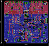
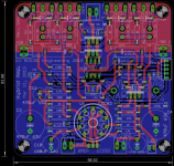
After several mails exchange with Hugh, we found that there could be several options depending of the MOSFET used in the driver stage, therefore I have designed two PCB versions to test them...
The rev. 5 is the original version but with a Depletion MOSFET and different possibilities of capacitors / resistors mounting while the Rev. 5HD is Hugh Dean variation with a enhancement MOSFET and a Mu-follower stage.
I am waiting for the PCB to test them 🙂
Rgds,
Marc
Attachments
hi marc,
waiting for your build. I think it is much better if you start a new thread for this hybrid amp.
regards,
dacz
waiting for your build. I think it is much better if you start a new thread for this hybrid amp.
regards,
dacz
Looks good, I'd be interested in hearing how the tests go.
Are the Fets unobtainium - Do you have a source figured out for them yet?
Are the Fets unobtainium - Do you have a source figured out for them yet?
Hi Everybody,
Just a quick message to inform you that the PCB send from China two weeks ago are still in Beijing 😡 I have contacted PCBWay and their only repeated answer is that E-packet is not stable and they suggest to use DHL, why do they offer E-packet on their web site in this case ? I have used DHL once at the beginning, but for a 20 $ order of PCB, it cost me 25 $ of freight therefor the total exceeded 40 $ (the maximum without VAT) and I had to pay 20% of VAT = 9 $ but DHL added 16 $ of administrative fee to collect these 9 $... Result : I have paid 50 $ of freight + taxes + fees for an order of only 20 $
I have now asked to PCBWay to solve the problem quickly without asking me to pay more, I was very positive for them until now, but I am now quite disappointed, the good solution should have been to make an other batch and to send it ASAP !
I will start the new thread on the hybrid amplifier when I will receive the boards, should I put it in the tubes or the semiconductors forum ?
Best regards,
Marc
- Home
- Amplifiers
- Solid State
- Very simple quasi complimentary MOSFET amplifier