Haha that's ok, I assume I can just program it again with the same steps? Hopefully I can program it while it's plugged into the B2B connectors, because I'm scared to pull it out. It was a tight fit.
EDIT: I left the switches in their stock configuration, A and B on, C and D off. Is that correct?
EDIT 2: The switch C change, that lights up the settings without the random button being pressed: does that defeat the purpose of the Random setting?
EDIT: I left the switches in their stock configuration, A and B on, C and D off. Is that correct?
EDIT 2: The switch C change, that lights up the settings without the random button being pressed: does that defeat the purpose of the Random setting?
Last edited:
Yes, you can program it again with the same steps. Although I usually remove it, I think I also programmed it once or twice while it's plugged into the B2B connectors.
There used to be a "known issues" document somewhere on the Trenz website stating that you have to switch off switch 1 for reliable start up, or switch 2 when you need the USB interface. I think I switched off both 1 and 2, and that didn't work.
Switches 3 and 4 just affect the way the lamps work. I don't think switching switch 3 on defeats the purpose, because the lamps still turn off when you put the rotary switches in the "surprise" position and don't push the button. That is, they only turn on during the A, B and C choices of the ABCX test, or when the button is pushed.
From reading this, I think Switch 1 might not matter and 2 should be on? Since the USB bus isn't used for power?
"Switch 1 (S1A) is used to connect the USB controller to the I2C serial EEPROM.
When S1A is "ON", serial I2C EEPROM is connected to the USB controller,
when switch is "OFF", the USB controller is disconnected from the EEPROM4.
Turn S1A off when programming the USB EEPROM (storing the USB vendor ID
and device ID). This will force the USB controller to provide its default vendor ID
and device ID.
Switch 2 (S1B) is used to control DC-DC converters. When switch is "OFF",
converters are controlled by the USB controller. When switch is "ON",
converters are enabled regardless of USB controller actions. At start-up, the
USB controller switches off 1.2V, 1.5V and 2.5V power rails and starts up the
module in low-power mode. After enumeration, the USB controller firmware
switches the 1.2V, 1.5V and 2.5V power rails on, if enough current is available
from the USB bus."
This was the known issue, I don't know if it is still on the Trenz website or if they fixed it when they revised the modules a couple of years ago:
"TE0630 Known Issues
Created by Sergio Pavesi, last modified by Oleksandr Kiyenko on 10 12, 2014
Possible race condition during power up
S1B and S1A both set to ON can lead to a race condition. When Bitgen option "reset_on_error" is not set, the module does not boot.
Explanation
When S1B switch is ON, FPGA and FX2 start at the same time and as S1A is also ON, FX2 runs custom firmware which initializes SPI and trying to switch ON FPGA power (which is already forced to ON by S1B). So FX2 create error during FPGA load. As "reset_on_error" is not set FPGA will not try to boot again.
Solutions
1. If you don't use our USB API, switch S1A to OFF (S1B to ON). This way you disable FX2 activity on SPI bus and FPGA will boot from SPI by power on. (Fastest boot)
2. If you need USB API.
Switch S1B to OFF (S1A to ON). This way FX2 firmware will control FPGA power and FPGA will be powered up and start boot only after full FX2 initialization.
Enable "reset_on_error" option for bootstream generation. This way, even if S1B is on and FX2 SPI init and FPGA boot will be in the same time (and bitstream will be corrupted during transfer by SPI) FPGA will reboot again if error occur.
Init and boot time depend on board capacitance and power supply so may vary from board to board, which affect to boot behavior."
Anyway, switch 2 on and switch 1 off should work.
Attached is the source code for the version of post #1519, just in case anyone would want to make their own variant.
The FIR filters and FIFOs were generated in the same way as for the earlier versions, except that the optimization target for the filters was set to "timing" rather than "area", the five times interpolating filter is no longer required and the three times interpolating filter firint3 is shorter and has a different coefficient set, interpolfir3_version3.coe.
The synthesis and implementation settings are the same as in the documentation of version 1, except that register_balancing was set to "yes" instead of "forward". Implementation resulted in a couple of timing errors that I looked at and judged not to be problematic. In fact most of them relate to a path that I had tried to put a timing ignore constraint on.
Attachments
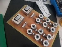
Got the Jensen transformers and my input PCBs in today. All that's left is power transformers and the FPGA.
Hi please point to the schematic for analog filter (with interstage transformer PCB) ?
Thanks 🙂
Attachments
Last edited:
Bought 3 matched pairs of Philips JAN 6922. Got them for $130, most other options were pretty expensive. I want to get the DAC functional before dumping money into tubes.
Premium Matched PAIR of JAN 6922 / 6DJ8 ECC88 Philips ECG USA Valve Tubes - NOS | eBay
Premium Matched PAIR of JAN 6922 / 6DJ8 ECC88 Philips ECG USA Valve Tubes - NOS | eBay
Marcel,
Any tips for first time fire up of the ValveDAC? I'm about ready to press the switch with just the cable to the recpnstruction filter to be made. Should get to in this week I hope.
With a point-to-point build I would go through in stages checking voltages before putting in valves and then re-checking but this build is more complicated. Does the FPGA need to be in place for first startup?
Cheers,
Anthony
You finished your build? I'm waiting on my custom transformer from Toroidy, then I'm ready to go. What are you doing for the cases?
Just bread boarding for now. Will build the case/s when the time comes. There are several things to experiment with first before final case layout can be determined.
Marcel,
Any tips for first time fire up of the ValveDAC? I'm about ready to press the switch with just the cable to the recpnstruction filter to be made. Should get to in this week I hope.
With a point-to-point build I would go through in stages checking voltages before putting in valves and then re-checking but this build is more complicated. Does the FPGA need to be in place for first startup?
Cheers,
Anthony
If I were to build a second one, I guess I would first test the digital part. There are quite a few things that can go wrong on the digital side, hand soldering 0.5 mm pitch components for example, or wrong DIP switch settings on the FPGA board, or forgetting to short the R102 pads on the FPGA board - although in your case I already did that for you. It is nice when you can debug those things without potentially lethal voltages.
When you only apply the 5 V supply and a digital input signal, you should get sigma-delta modulates at the outputs of U11. You can functionally test those with a low-pass filter, like the one described in post #369, https://www.diyaudio.com/forums/dig...-linear-audio-volume-13-a-37.html#post6016188
I bought the WaveIO, which has data, word clock, bit clock, master clock, Vin, and 5 GNDs. I think to connect to P9, it's:
data to pin 5
word clock to pin 11
bit clock to pin 9
master clock to nothing
Vin to pin 19 or 20
GND to pins 2, 4, 6, 8, 10?
I think I forgot to reply to this post. Assuming the WaveIO requires a 3.3 V supply from the valve DAC and that there is PCM or DoP coming out, it's all correct, but there are a few other things needed:
P9 pin 1: needs to be pulled down when you use the I2S input, otherwise the DIX4192 inputs are used and the I2S signal on P9 is ignored. It can be connected to an extra contact of the source selection switch if you want to use P9 and the DIX4192 inputs.
P9 pin 3: has to be pulled down to ground, otherwise the signal from P9 gets muted
I'd shift the ground connections to pins 4, 6, 8, 10, 12, or just connect all of them (2, 4, 6, 8, 10, 12, 14).
I had planned on connecting P9-1 to my source selection switch. Should I connect P9-3 as well, since the selector switch is connecting to ground?
And although the WaveIO supports DSD, I only plan on using PCM.
And although the WaveIO supports DSD, I only plan on using PCM.
The intention was for P9 pin 3 to be connected to the mute output of whatever drives P9 if there is such a mute output, and to be connected straight to ground otherwise. You can also connect it to the switch contact, the time until you get sound after switching to the I2S input will then be about 18 ms longer.
There is no harm in leaving it connected to ground indefinitely? I thought it might need to be muted when not in use, such as if I'm using optical input.
If I were to build a second one, I guess I would first test the digital part. (...)
When you only apply the 5 V supply and a digital input signal, you should get sigma-delta modulates at the outputs of U11.
Sorry acg, I've been so stupid! This can't possibly work for the original valve DAC because it needs the 27 MHz valve crystal oscillator and the signal indicating that the 85A2 has ignited!
- Home
- Source & Line
- Digital Line Level
- Valve DAC from Linear Audio volume 13