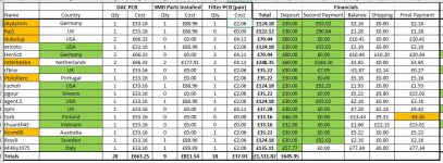
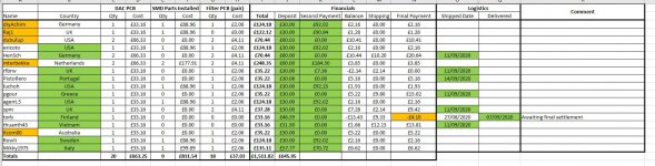
Having exchanged PMs with Mikky1975 we have clarified his requirements and I have adjusted the GB spreadsheet accordingly.
As it turns out he only wants one PCB so I have one left if there are any more lurkers out there? I won't be running another GB so this may be the last opportunity.
Also, an apology - in slotting Mikky1975 into the spreadsheet I realised that I had omitted to include the cost of the smd stencil so the figures for the smd soldering service have increased a little - sorry about that.
Attachments
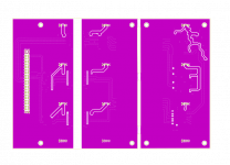
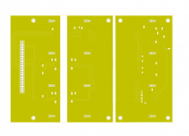
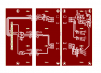
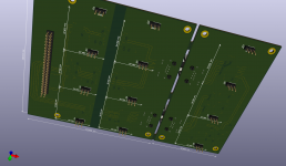
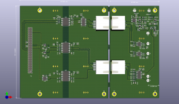
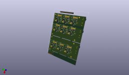
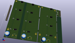
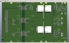
Having spent a bit of time laying out the boards last couple weeks, this is what I have so far. A 4 layers pcb for the isolators and a separate 2 layers power supply board, that the isolator pcb can plug onto. I may have gone a bit crazy on the via fences. But this is what Analog does on the EVM. So, I just copy it. In addition to revised schematics, based upon Marcel's advices, I have the 3D renderings of the top and bottom of the two pcbs, and separate printouts of each copper layers. On the 4 layers board, the inside layer 1 is ground and insider layer 2 is power. But, it is mostly ground anyway, as I used traces instead of a pour. I also did a little adapter board to P13. Suggestions?
Attachments

Last edited:
There are more files of the power supplies.
Attachments
Last edited:
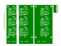
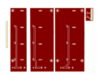
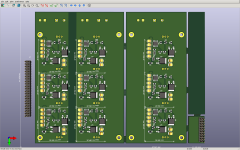
Boards arrived today.
Look very good.
Now the fun begins!
Thank you.
Simon
Great. Have fun.
...this is what I have so far.
Interesting. 😎
I've only had a quick look at your attacments and sorry if this has been covered before; I don't see any oscillators?
What sort of separation distance (i.e. Ethernet cable length) between the two boards are you envisaging?
Correction: Ah, I see, external oscillators via J10 & J11
Last edited:
The boards I posted last week should be landing very soon.
Boards turned up monday morning. Thanks and much kudos to you and MarcelvdG.
Interesting. 😎
I've only had a quick look at your attacments and sorry if this has been covered before; I don't see any oscillators?
What sort of separation distance (i.e. Ethernet cable length) between the two boards are you envisaging?
Correction: Ah, I see, external oscillators via J10 & J11
I plan on getting a couple well tempered clocks from Andrea's group buy. It is looking likely to be two clocks, plus two frequency doublers, in 4 separate boxes. I read that LVDS can do long distance. See
https://www.ti.com/lit/an/slla127/slla127.pdf
But, all I really want is to separate the BBB maybe 500mm from the DAC.
Last edited:
I read that LVDS can do long distance.
IIRC, Twisted Pear say their Teleporter has been tested over 30metres.
Will watch your development with interest.
Thanks for your interest. I'm still making minor adjustments here and there. I will order boards, solder them. If it works, and I think it will, then I will post gerber and bom here, so others can play with it, if they want. As there is minimum quantity for a pcb order, and I really only need one set, I should have extra as well.
I plan on getting a couple well tempered clocks from Andrea's group buy.
I started to check out Andrea's threads but they're in a really confused state and I haven't yet found a 'picture' of what is on offer with the various options. I assume you'll be using a 22/24MHz oscillator pair for the potential to use DSD512?
'Sale' of the very last DAC PCB pending.
The last PCB is still available.
I started to check out Andrea's threads but they're in a really confused state and I haven't yet found a 'picture' of what is on offer with the various options. I assume you'll be using a 22/24MHz oscillator pair for the potential to use DSD512?
more likely a 11MHz/12MHz Drixo PCB pair, plus 11MHz/12MHz SC cut crystals, plus a 11 to 22MHz and a separate 12 to 24MHz frequency doublers. The information is spread out over two separate threads, and they decided not to publish schematics. So, it is confusing.
A construction with a frequency doubler could produce a spur at the second subharmonic of the 22.5792 MHz or 24.576 MHz clock, and if the DSD512 signal comes from a plain old single-bit sigma-delta, that could lead to artefacts due to mixing between the clock spur and the sigma-delta idle tone.
What level does the 11.2896 MHz or 12.288 MHz spur have compared to the 22.5792 MHz or 24.576 MHz? Can you say anything about what algorithm will generate the DSD512?
What level does the 11.2896 MHz or 12.288 MHz spur have compared to the 22.5792 MHz or 24.576 MHz? Can you say anything about what algorithm will generate the DSD512?
Last edited:
well, I have not seen the frequency doubler schematic, but it uses transformer. Andrea published some graphs
https://www.diyaudio.com/forums/dig...jitter-crystal-oscillator-53.html#post6339396
I can ask questions over there.
This post lists options and there are too many. The frequency doubler requires transformer(s). Maybe something likes this
Low Phase Noise Design: Frequency Multipliers
But they decide not to publish schematic, so can't say for sure until I can see high res pictures.
Last edited:
- Home
- Source & Line
- Digital Line Level
- Valve DAC from Linear Audio volume 13