The first Valve DAC GB PCB (my spare from the original purchase) is on its way to torb in Finland today.
Sweet! Thanks Ray!
You're very welcome, I hope you enjoy the project as much as I have.
Please report back on you build progress and listening impressions (eventually!).
Ray
Please report back on you build progress and listening impressions (eventually!).
Ray
Please comment on my attached pdf schematic. It is version of PPY's isolator/reclocker for only the Valve DAC. Marcel, do you think it works?
I include links to datasheets.
ADuM110N
https://www.analog.com/media/en/technical-documentation/data-sheets/ADuM110N.pdf
ADuM130D
https://www.analog.com/media/en/technical-documentation/data-sheets/ADuM130D_130E_131D_131E.pdf
PO74G14A
http://www.potatosemi.com/potatosemiweb/datasheet/PO74G14A.pdf
PO74HSTL85352A
http://www.potatosemi.com/potatosemiweb/datasheet/PO74HSTL85352A.pdf
LM317L
https://www.ti.com/lit/ds/symlink/lm317l.pdf
TL1431
https://www.ti.com/lit/ds/symlink/tl1431.pdf
Attachments
Last edited:
=)
I will report back, but I am not a fast builder=)
Tor-björn
I will report back, but I am not a fast builder=)
Tor-björn
You're very welcome, I hope you enjoy the project as much as I have.
Please report back on you build progress and listening impressions (eventually!).
Ray
Hi Agent.5
I think that sch is conceptually OK?
0. PO74G14A is inverter and PO74HSTL85352A expects in-phase sygnal? I think that You have inverted MCK at he output? So consider to add one more inverter at the input OR use negative out from MCK IC selector.
BUT it will be better for my opinion to use balanced outputs form the IC. AND use differential receiver to make Single ended sygnal just before place when You need?
1. I think that You can use better current limiter for shunt reg TL431. Not that with 317.
Other thing about regs, if You supply shunts from 5V to 3.3V that will be 1.7V for pass device before shunt elemement. That could be too low? For Darlington pass element in current limiter module about 2.7V is some minimum? Anyway I will post better current limiter-before-shunt also simple circuit.
2. Put signal integrity resistors in every pcb line between the ICs. Not partially only. In that way You will have an option to use them or not to use.
3. Also on the PCB put some R (or L) element before decoupling caps at each IC. That will include option to use RC or LC HF filter OR NOT to use when populated with 0R or shorten. Also it is less complicated to measure current consumption on every IC with specific working Fo and real PCB on that place for R or L element with current meter directly... For choosing proper value of shunt current that should be minimum 120% of IC consumption.
4. Place shunt element close to the IC.
5. Please check for the thermal and max power of 431 element You will use? That isolators will consume more current as frequency is higher. I think I have some measurements of current for these classic Fo?
.
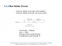
Just one thing these 2 x 100K resistors (at the inputs of inverters) attenuate signal? Or they are bus holders?
I think that sch is conceptually OK?
0. PO74G14A is inverter and PO74HSTL85352A expects in-phase sygnal? I think that You have inverted MCK at he output? So consider to add one more inverter at the input OR use negative out from MCK IC selector.
BUT it will be better for my opinion to use balanced outputs form the IC. AND use differential receiver to make Single ended sygnal just before place when You need?
1. I think that You can use better current limiter for shunt reg TL431. Not that with 317.
Other thing about regs, if You supply shunts from 5V to 3.3V that will be 1.7V for pass device before shunt elemement. That could be too low? For Darlington pass element in current limiter module about 2.7V is some minimum? Anyway I will post better current limiter-before-shunt also simple circuit.
2. Put signal integrity resistors in every pcb line between the ICs. Not partially only. In that way You will have an option to use them or not to use.
3. Also on the PCB put some R (or L) element before decoupling caps at each IC. That will include option to use RC or LC HF filter OR NOT to use when populated with 0R or shorten. Also it is less complicated to measure current consumption on every IC with specific working Fo and real PCB on that place for R or L element with current meter directly... For choosing proper value of shunt current that should be minimum 120% of IC consumption.
4. Place shunt element close to the IC.
5. Please check for the thermal and max power of 431 element You will use? That isolators will consume more current as frequency is higher. I think I have some measurements of current for these classic Fo?
.
Just one thing these 2 x 100K resistors (at the inputs of inverters) attenuate signal? Or they are bus holders?
Last edited:
Please comment on my attached pdf schematic. It is version of PPY's isolator/reclocker for only the Valve DAC. Marcel, do you think it works?
The ground pin of U1 is connected incorrectly, but when that is fixed, I don't see any reason why it wouldn't. You may need termination resistors at the clock and data outputs if the lines to the raw DSD valve DAC are not very short. I haven't made any attempt to check the timing yet. I'm not sure if the split digital ground with L2 is a good idea, usually you want return currents to flow in as small a loop as possible.
Yes. The clock buffer outputs inverted square waves. I can use its negative output instead. The Valve DAC has a u.fl connector for MCLK. My thinking is to use a 200mm pre-made u.fl cable to connect the isolator to the DAC. Doing a all-in-one-box solution, I prefer to send a single-end signal out. I am also researching other single-end clock buffer (with and without enable and fanout).0. PO74G14A is inverter and PO74HSTL85352A expects in-phase sygnal? I think that You have inverted MCK at he output? So consider to add one more inverter at the input OR use negative out from MCK IC selector.
BUT it will be better for my opinion to use balanced outputs form the IC. AND use differential receiver to make Single ended sygnal just before place when You need?
On the other hand, BBB is noisy and it is a good idea to keep it as far away from the DAC as possible. So, putting it in a separate metal box and send differential clock signal to a DAC in a separate box is very tempting. I am still thinking and any idea, suggestion, experiences are helpful and welcome.
Noted. Will recalculate voltage requirement and redo current source.1. I think that You can use better current limiter for shunt reg TL431. Not that with 317.
Other thing about regs, if You supply shunts from 5V to 3.3V that will be 1.7V for pass device before shunt elemement. That could be too low? For Darlington pass element in current limiter module about 2.7V is some minimum? Anyway I will post better current limiter-before-shunt also simple circuit.
Maybe, something like this
http://www.bristolwatch.com/ccs/img1/TL431_ccs_on.jpg
I may just use cascoded depletion CCS.
https://i.stack.imgur.com/NW6pz.png
Any suggestions?
Noted. Will add them to schematic2. Put signal integrity resistors in every pcb line between the ICs. Not partially only. In that way You will have an option to use them or not to use.
Noted. Will add LC filter to every chips. I will also spreadsheet current consumption of all the chips.3. Also on the PCB put some R (or L) element before decoupling caps at each IC. That will include option to use RC or LC HF filter OR NOT to use when populated with 0R or shorten. Also it is less complicated to measure current consumption on every IC with specific working Fo and real PCB on that place for R or L element with current meter directly... For choosing proper value of shunt current that should be minimum 120% of IC consumption.
Noted. My plan is to put all the high speed ICs on the top layer, and all the power supplies on the bottom layer. So, the shunt element will be no more than 3mm (1.6mm board + traces + empty space) from a +pwr pin. The PCB will connect to the BBB, offset to one side, and sit on an oversized heatsink. Look something like them4. Place shunt element close to the IC.
https://cdn.hardkernel.com/wp-content/uploads/2020/07/N2vsN2plussize1.jpg
https://ae01.alicdn.com/kf/H88b7bf8...near-Regulated-IN-1-8V-20V-OUT-0V.jpg_q50.jpg
any data that you have is welcome. I will research datasheet and spreadsheet out its current consumption5. Please check for the thermal and max power of 431 element You will use? That isolators will consume more current as frequency is higher. I think I have some measurements of current for these classic Fo?
Just one thing these 2 x 100K resistors (at the inputs of inverters) attenuate signal? Or they are bus holders?
I think they are just basic voltage divider to ensure that signal swings from the middle. I LT-spiced the circuit with 10K and without them. The sim result is the same. Maybe they are not needed. I got the idea from here
Waveform Conversion |
https://www.quora.com/How-is-a-square-wave-produced-from-sinusoidal-waveforms
Attachments
Last edited:
The ground pin of U1 is connected incorrectly, but when that is fixed, I don't see any reason why it wouldn't.
Noted. Also, all the talks about ground bounce and so many things that I do not understand over at that clock thread makes me feel that using a many channels IC and then trying to ground a bunch of unused channels is just not a good idea. I think that I will use two single inverter gate 74x1G14, one for each channel, instead.
You may need termination resistors at the clock and data outputs if the lines to the raw DSD valve DAC are not very short. I haven't made any attempt to check the timing yet.
Noted. Will add 50 ohms resistors at clock and data outputs and clock inputs.
I'm not sure if the split digital ground with L2 is a good idea, usually you want return currents to flow in as small a loop as possible.
I got the idea here, where marce was helping to design an usb isolator
DIY USB isolator
Last edited:
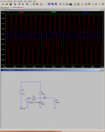
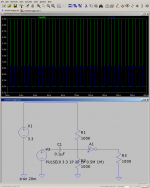
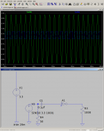
I found some circuit that is recommended for sine to square module. It is a like inverter input stages before selector on the schematic. There are some differences in value of elements. Here is the PDF (if it repeated PDF sorry...)
Consult with the Marcel about values? These 100nF of Input C is maybe too much? And in the PDF value of R at the input of the inverter are 51K.
...
I think That maybe is better to use somehow separate inverters for each MCK signal? Because they are present at the the same time in same IC?
It will be ideal to find just double inverter package IC. One inverter for the input and other for same rising/falling edge like at the input? OR use 2 X potato '14 chip? And If they 2xR acting like sort of bus holders maybe rest of 2 inverters per IC could be use like bus holders (week keaper)?
...
Attachments
Agent.5
"Yes. The clock buffer outputs inverted square waves. I can use its negative output instead. The Valve DAC has a u.fl connector for MCLK. My thinking is to use a 200mm pre-made u.fl cable to connect the isolator to the DAC. Doing a all-in-one-box solution, I prefer to send a single-end signal out. I am also researching other single-end clock buffer (with and without enable and fanout).
On the other hand, BBB is noisy and it is a good idea to keep it as far away from the DAC as possible. So, putting it in a separate metal box and send differential clock signal to a DAC in a separate box is very tempting. I am still thinking and any idea, suggestion, experiences are helpful and welcome."
first I think that these 200mm are long for single ended type of connection? from quick calc 1m of some sheilded cable has 70-80pF per 1m typicaly, capacitance + must include capacitance on the soldering at the conn? that is minimum 15pF + via SE line?
.
Ballanced connection will be maybe better solution? In that way You can make simple PCB with diff. receivers close OR at the PCB input DAC jacks. Please consult with Marcel about this idea?
.
{From my (personal sound taste) I used many times diff. transmitter/receiver for all digital bus inside DAC in shorter lines and sound was better than with SE lines.}
.
One important thing - If You are think to employ balanced line transmitter/receiver with ENABLE option, You can avoid complex selector IC? Selection of which clock running remains the same with enable pins. (must be applied same on the transmitter and on the receiver for same line.)
unfortunately, Potato has neither single nor dual chips, and only sell 6 packs. I agreed that having a separate inverter for each MCLK is better.
There are single schmidtt
inverted
https://assets.nexperia.com/documents/data-sheet/74LVC1G14.pdf
and
non-inverted
https://assets.nexperia.com/documents/data-sheet/74LVC1G17.pdf
But, they are really really tiny. It may or may not be a problem, as I imagine this board will be hot-air soldered.
I think the converter design is fine. The values of the resistors and input capacitors probably need changes. 47pf and 51K sound good.
One important thing - If You are think to employ balanced line transmitter/receiver with ENABLE option, You can avoid complex selector IC? Selection of which clock running remains the same with enable pins. (must be applied same on the transmitter and on the receiver for same line.)
I thought about it. I will do some research and draft a schematic so we can look at it.
Noted. Also, all the talks about ground bounce and so many things that I do not understand over at that clock thread makes me feel that using a many channels IC and then trying to ground a bunch of unused channels is just not a good idea. I think that I will use two single inverter gate 74x1G14, one for each channel, instead.
I can't think of any harm done by unused CMOS gates as such, as long as all unused inputs are either grounded or connected to the supply. The only disadvantage of a many channels IC of which only one channel is used is that it will usually have a bigger package than a single channel IC, and the bigger the package, the longer the connections from the chip to the outside world (including supply and ground connections), and the more inductance they have.
Noted. Will add 50 ohms resistors at clock and data outputs and clock inputs.
Are the oscillators designed to drive a 50 ohm load?
For CMOS digital outputs, I usually take the characteristic impedance of the line that has to be driven, subtract an estimate of the output resistance of the driving gate, round what is left to the nearest E12 value and use that for the series resistor. I estimate of the output resistance of the driving gate by looking up in the datasheet how much the output voltage changes with output current. Hence, I usually end up using 33 ohm or 39 ohm for 50 ohm lines.
It's not quite the same situation, as that circuit uses differential signals only, so the return currents are supposed to flow in the other branch of the differential connection rather than through the ground plane.
I can't think of any harm done by unused CMOS gates as such, as long as all unused inputs are either grounded or connected to the supply. The only disadvantage of a many channels IC of which only one channel is used is that it will usually have a bigger package than a single channel IC, and the bigger the package, the longer the connections from the chip to the outside world (including supply and ground connections), and the more inductance they have.
Noted.
Are the oscillators designed to drive a 50 ohm load?
yes. 50 ohm, per Andrea_Mori. He suggested to "add a 50 ohm resistor at the input to load the oscillators."
It's not quite the same situation, as that circuit uses differential signals only, so the return currents are supposed to flow in the other branch of the differential connection rather than through the ground plane.
Thanks. Will eliminate split ground.
Last edited:
By the way, those isolators have a maximum delay of 14 ns at 3.3 V +/- 0.3 V. There is one in the path from the clock generator to the Beagle Bone Black and one in each data path back. With the 5 ns set-up time of the raw DSD valve DAC, that brings the total to 2 * 14 ns + 5 ns = 33 ns. The clock period is at least 1/24.576 MHz ~= 40.69 ns, so that leaves 7.69 ns - the skew of U6 for the Beagle Bone Black assuming that everything is clocked on the same clock edge (no opposite-edge clocking) and that delays in wiring are negligible. The skew of U6 is only 30 ps max, so that's 7.66 ns. Does anyone know if 7.66 ns suffices?
Last edited:
In a similar situation, I used a single box, but split it horizontally with a sheet of grounded 2 sided copper pcb stock. That way, easy to mount noisy stuff like BBB on one side and clean stuff on the other side. Signals connected with ufl. This way it's easy to isolate the noisy stuff but also keep ufl cables short. For me, thinking in 3D was an epiphany.On the other hand, BBB is noisy and it is a good idea to keep it as far away from the DAC as possible. So, putting it in a separate metal box and send differential clock signal to a DAC in a separate box is very tempting. I am still thinking and any idea, suggestion, experiences are helpful and welcome.
I used a single box, but split it horizontally with a sheet of grounded 2 sided copper pcb stock. ... For me, thinking in 3D was an epiphany.
Good idea. I am really considered putting BBB and whatever this thingy that I ended up with in its own metal box regardless. If it is just a box inside another box, then I can drill a few hole and let the u.fl cables through. Even if I use 100mm or 150mm cable, the DAC will be close to the BBB.
I am doing research on the LVDS transmitter/receiver idea. It is doable. Twist Pair sells a similar product named "The Teleporter Digital Transceiver." So, it has been done. We need more than 4 channels here and require a bit of enable logic. However, it will add ns to the data chain. I feel like I am inside an episode of 24, when Jack Bauer keeps yelling that we are running out of time. Maybe we need to drop down to DSD256 so we get another 40ns or so for a pint.
Last edited:
I also talked to the Potato chip people. Unused connections need to be terminated with dummy capacitor load and should not just do a not connect. "If you know the size of your nQ0 & nQ1 loading capacitors, you use the same loading capacitor as dummy.
If you do not know, then use 8pf for dummy."
If you do not know, then use 8pf for dummy."
Last edited:
Hi Agent.5
"hand made" oscillators usually already have some sine to square module at the output? Please check with Your oscillator sch. Maybe it is not a good thing to repeat 2 X same circuit?
"hand made" oscillators usually already have some sine to square module at the output? Please check with Your oscillator sch. Maybe it is not a good thing to repeat 2 X same circuit?
- Home
- Source & Line
- Digital Line Level
- Valve DAC from Linear Audio volume 13