Hi Marcel, that's really positive, thanks. I'll be happy to have a go at building one (and before anyone asks why, because I can).
On thinking about it, is the isolator/reclocker actually relevant as everything it does is invisible to the DAC? Should it not just be sufficient to know that to input to the DAC there are signals for DSD_Left, DSD_Right, DSD_Clock and also Master Clock (along with DSD_On and Mute flags - important for managing extraneous loud pops when data rates change). The reclocker will have taken care of selecting the correct clock oscillator depending on whether it is receiving 44.1 or 48KHz based data.
ppy's website does seem to be a bit hit and miss regarding access. I often get timeout errors but then suddenly it works fine. I think I have the schematics etc. downloaded from his site and I can send them to you if it helps?
Thanks again.
Ray
It's a pity because I never understood how reclocking is supposed to work.
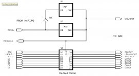
Please see attachment below from Iancanada McFIFO manual. The FIFO MCLK may be also be routed back to the USB board either as-is or divided down to a lower frequency, as required. In the case of Cronus, it looks very similar, but without a FIFO FPGA.
Sometimes, two stages of D-flip flops are used.
Attachments
Last edited:
On thinking about it, is the isolator/reclocker actually relevant as everything it does is invisible to the DAC? Should it not just be sufficient to know that to input to the DAC there are signals for DSD_Left, DSD_Right, DSD_Clock and also Master Clock (along with DSD_On and Mute flags - important for managing extraneous loud pops when data rates change). The reclocker will have taken care of selecting the correct clock oscillator depending on whether it is receiving 44.1 or 48KHz based data.
OK, then I just make a raw DSD interface and leave any reclocking to the reclocking board.
Please see attachment below from Iancanada McFIFO manual. The FIFO MCLK may be also be routed back to the USB board either as-is or divided down to a lower frequency, as required. In the case of Cronus, it looks very similar, but without a FIFO FPGA.
Sometimes, two stages of D-flip flops are used.
Thanks for the explanation! It makes sense when the USB board gets (a derivative of) the reclocker clock and can adjust its data rate to it.
Thanks for the explanation! It makes sense when the USB board gets (a derivative of) the reclocker clock and can adjust its data rate to it.
Yes, that is what the TPA Hermes/Cronus does; the Beaglebone Black (BBB) receives a masterclock input so that it runs at the rate of the incoming data. 'Out of the box' the BBB only has a single cheap (48KHz data) oscillator so would have to resample incoming 44.1KHz data.
It makes sense when the USB board gets (a derivative of) the reclocker clock and can adjust its data rate to it.
Yes, the better USB boards can accept external clocks, and also output a logic signal to tell the clock board which clock family (44/48) it needs for the current USB audio being received.
OK, then I just make a raw DSD interface and leave any reclocking to the reclocking board.
An 'all in one board' woud be very nice but I think it is too much to expect of you and anyway, having just a raw DSD interface gives more flexibility, especially as the project is experimental.
Hi again Marcel. I've been rereading your Linear Audio document and in section 5 you talk about potential clock issues, for example;
"The CD sample rate and its multiples will be particularly troublesome, because the ratio of 28.224 MHz to 44.1 kHz is a multiple of 64. An SPDIF or AES/EBU interface typically has spectral peaks at the 32nd and 64th harmonics of the audio sample rate, see figure 3.5 of reference [27]. Similarly, an I2S interface often has a bit clock running at 64 times the sample rate. Relatively low (and therefore strong) harmonics of these frequencies can then cause trouble."
If DSD audio and clock data at, say DSD256 or DSD512, are input to the core of your DAC might there be an issue?
Ray
Last edited:
Sorry Marcel, more questions/requests...
Ray
- If you're already substantially reworking the PCB for DSD only, might you consider stripping it back further to just the core of your DAC. For example, taking off some or all of the power supply sections; apart from reducing the footprint/cost, this would also give more flexibility to subsequently try, say, alternative power supply arrangements (such as different regulated supplies). In some ways such flexibility might help builders interested in a PCM version, but deterred by the cost of the original board, by making it more modular?
- Could you include ufl connectors for the DSD data/clock inputs? A standard 2.54mm pitch header will be fine for the DSD_on/Mute connections.
- If the board is circa 1.6mm thick, could a few additional stand-off holes be included close to the valves/tubes to reduce board flexing when inserting/removing valves/tubes.
- Would it be appropriate to consider ppy's transformer based output stage in place of you own reconstruction filter board?
Ray
Last edited:
Hi again Marcel. I've been rereading your Linear Audio document and in section 5 you talk about potential clock issues, for example;
"The CD sample rate and its multiples will be particularly troublesome, because the ratio of 28.224 MHz to 44.1 kHz is a multiple of 64. An SPDIF or AES/EBU interface typically has spectral peaks at the 32nd and 64th harmonics of the audio sample rate, see figure 3.5 of reference [27]. Similarly, an I2S interface often has a bit clock running at 64 times the sample rate. Relatively low (and therefore strong) harmonics of these frequencies can then cause trouble."
If DSD audio and clock data at, say DSD256 or DSD512, are input to the core of your DAC might there be an issue?
Ray
The part you are quoting applies to systems with asynchronous sample rate conversion, they should preferably not have a clock frequency that is at or very close to a multiple of the usual audio sample rates. As the native DSD version will not have any sample rate conversion at all, this doesn't apply.
A crosstalk issue that all systems based on sigma-delta modulation have is crosstalk from the sigma-delta modulate to the clock or to the voltage or current reference. This causes intermodulation products between out-of-band quantization noise and out-of-band quantization noise, which will raise the in-band noise floor and possibly cause in-band tones. For that reason your suggestion to use U.FL coaxial connectors is a very good idea.
Sorry Marcel, more questions/requests...
Thanks
- If you're already substantially reworking the PCB for DSD only, might you consider stripping it back further to just the core of your DAC. For example, taking off some or all of the power supply sections; apart from reducing the footprint/cost, this would also give more flexibility to subsequently try, say, alternative power supply arrangements (such as different regulated supplies). In some ways such flexibility might help builders interested in a PCM version, but deterred by the cost of the original board, by making it more modular?
- Could you include ufl connectors for the DSD data/clock inputs? A standard 2.54mm pitch header will be fine for the DSD_on/Mute connections.
- If the board is circa 1.6mm thick, could a few additional stand-off holes be included close to the valves/tubes to reduce board flexing when inserting/removing valves/tubes.
- Would it be appropriate to consider ppy's transformer based output stage in place of you own reconstruction filter board?
Ray
I'll see what I can do. I want to keep the filter separated from the main board for reasons of cost, but also to make experimenting with different variants easier. The first filter capacitor will have to stay on the main board, though, so most of the high-frequency currents stays in a small loop.
I'll see what I can do.
Thank you Marcel. I'm getting quite excited about this project as it'll be good to try breakng some new ground. I'm also very grateful that you're prepared to help at all so I don't want to create a burden for you by asking too much so, please, don't do anything beyond what you consider reasonable, for example, if it's simpler to leave the power supply arrangments as they are that'll be fine as I can always find a suitable place to bypass them if I want to experiment later. I also bow to your far superior knowledge on what is the most appropriate technical configuration.
Cheers
Ray
Last edited:
See the attachment for a schematic proposal for a raw-DSD-only version. There are some components that may need tweaking, especially for DSD512, but I'll get back to that. I tried to stay as close as possible to the original to get the best chance that it will work. I left in the power supply section because it is so intertwined with the mute circuit.
C28, C29, C50 and C51 have to be changed depending on the chosen output filter. I don't really know what filter is most suitable for DSD. With its bandwidth of more than 80 kHz, the original filter is probably too wide for the lower DSD rates and its smooth roll-off can't be corrected for. Maybe a third-order Butterworth just above 40 kHz?
C28, C29, C50 and C51 have to be changed depending on the chosen output filter. I don't really know what filter is most suitable for DSD. With its bandwidth of more than 80 kHz, the original filter is probably too wide for the lower DSD rates and its smooth roll-off can't be corrected for. Maybe a third-order Butterworth just above 40 kHz?
Attachments
Thanks Marcel and sorry for not following up sooner but its proving to be a busy week.
The only thing that has caught my eye is that you don't seem to be using the DSD_ON flag - is it needed in the event of PCM data being accidentally sent to the DAC - I'm assuming that's why it's used on the DSC2 projects?
I'll put some time aside this evening to look through the schematics properly.
You can find the DSDON input on the page with the supply and mute control circuitry. By the way, I've added a few pull-down resistors on the clock, data, MUTE and DSDON inputs to keep things from floating when the source is not connected.
Apologies Marcel, in my hasty first scan I missed the DSD_ON.
I'll be having a more considered look this evening but my initial feeling is ' lets build one!'.
I'm thinking that as it isn't too far removed from your original valve DAC conceptually (essentially it's the same decoder engine, just without the front end fot processing PCM data) it should be low risk in terms of making it function and for sound quality aspects we'll have to wait and see/hear.
Your separate filter board now makes a lot of sense as it allows simple experimentation with different output arrangements.
Hi Marcel. I've spent an hour or two perusing the schematics. I don't pretend to understand all of it but I think I've succesfully followed the logic for the clock and data elements. I understand why it works to keep the power supply from your earlir schematics.
A couple of suggestions;
I like the option of using regulated DC supplies for tube filaments. Could you include an option to disconnect F1 & F2 with an option to connect up a DC supply. Not a big issue but I've always that DC regulates heaters are generally quieter,
Just thinking about keeping everything flexible with respect to the output filter. Could C28, C29, C31 & C32 be moved (schematically/logically) after Q1, Q2 & Q3 and actually left off the DAC core board? I know you say the caps need to be close to the output of the DAC core but my thinking is to relocate them to a separate filter board but to arrange things so the filter board stacks closely under the core board, retaining the short track routing but allowing easy experimentation with the output filters, plus, reducing the size of the PCBs so saving cost and estate space? The DAC core board could use a suitable PCB header arrangement on it's output to enable close coupling and swapping filter boards wouldn't need compontnets to be repositioned/replaced/resoldered.
Let's build one!
Hi Ray,
The supply transformer actually has a connector as footprint and the fuse and switch have no footprint at all. That is, I've used a dirty trick to draw off-board components in the schematic without having to put them on board. As a result, you can already connect a DC heater supply instead of a transformer if you like. Mind you, the average of the heater voltages is pulled to about -250 V with respect to ground to reduce the voltage across the heater to cathode insulation, so make sure you can't touch the heater supply (but the same holds for a heater transformer winding).
Moving C31 and C32 after Q1, Q2 and Q3 is not a good idea, because the common-mode voltage at the output of the E88CCs would turn on the JFETs unintendedly (and if it didn't, it would blow them up). An alternative might be to leave C31 and C32 as is, but to put a footprint for C28 and C29 on both the main board and the filter board.
Technically it is nicer to have them on the main board, but I can't predict how much difference it makes. With footprints on both boards you could try both variants and put them on the filter board if the difference is small.
Hi Ray,
The supply transformer actually has a connector as footprint and the fuse and switch have no footprint at all. That is, I've used a dirty trick to draw off-board components in the schematic without having to put them on board. As a result, you can already connect a DC heater supply instead of a transformer if you like. Mind you, the average of the heater voltages is pulled to about -250 V with respect to ground to reduce the voltage across the heater to cathode insulation, so make sure you can't touch the heater supply (but the same holds for a heater transformer winding).
Moving C31 and C32 after Q1, Q2 and Q3 is not a good idea, because the common-mode voltage at the output of the E88CCs would turn on the JFETs unintendedly (and if it didn't, it would blow them up). An alternative might be to leave C31 and C32 as is, but to put a footprint for C28 and C29 on both the main board and the filter board.
Technically it is nicer to have them on the main board, but I can't predict how much difference it makes. With footprints on both boards you could try both variants and put them on the filter board if the difference is small.
Thanks again Marcel.
You know far more about this design than I can ever hope so let's stick with your approach. All I ask is that you include some pads for a standard pitch (2.54mm) header to facilitate easy experimenting with output boards without the need to desolder connections (to avoid delaminating the copper tracks).
I'll wait for you to finalise the parts (you mentioned that in relation to usinfgDSD512 so presumably you're looking at frequency specs) and we can look to order a small number of PCBs. BTW, it would be really helpful to have silkscreens top and bottom as the boards will obviously need to be hand assembled so silkscreens with part numbers will help to avoid mistakes.
Quite excited now!
Ray
I've started to look at putting the output filter together as per Marcel's earlier recommendation but I also need a single-ended output so mulling over transformer options or maybe a John Broskie Glassware BCF board. The BCF board has pads for a simple first order LP filter so it might be possible to utilise them as part of the overall filter - have to check it out a bit more once I have a filter schematic.
Last edited:
- Home
- Source & Line
- Digital Line Level
- Valve DAC from Linear Audio volume 13