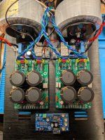
in the packet I bought I found an envelope with matched quad MOSFETs. This is a NOOB question, matched means NPN against the other NPN or is a matched pair NPN to PNP? Those MOSFET have a sticker on them but the marking do not match. I cant figure out you to pick them when I install them. I finally got a suitable chassis, I will post some pictures after I do some more work. The heatsinks are big for sure, almost 4kg each.
Heatsink dimensions 400/140/70. The plate itself is 14mm thick


any advice about my question in regards those those M1, M2 matched quad MOSFET? I would like to install and continue the build and I want to avoid a major mistake.
there is a bit of confusion on the markings in the BOM versus the PCB.
I am at the stage of installing MOSFET SJ313 and SK2013. These are the matched Quads I was talking about. I guess I will assume they are all matched and I dont have to somehow match an NPN with a PNP. The package I have for these MOSFET is entirely plastic, do I still need to place an insulator pad? I am guessing I dont need to place one and just place it directly on the radiator, this way I get a better heat transfer. I have Al oxide pads if still is recommended to use a pad.
I am at the stage of installing MOSFET SJ313 and SK2013. These are the matched Quads I was talking about. I guess I will assume they are all matched and I dont have to somehow match an NPN with a PNP. The package I have for these MOSFET is entirely plastic, do I still need to place an insulator pad? I am guessing I dont need to place one and just place it directly on the radiator, this way I get a better heat transfer. I have Al oxide pads if still is recommended to use a pad.
Eliad
I am not sure about confusion in the manual between PCB and BOM……this amp has been built by many peoples….( maybe 50 or so, maybe more since I have sold hundreds of PCBs…).
Matched Quad means NNPP all matched so no need to match on your side (unless the seller has sold you not what you paid for…). There is a test procedure in the manual to draw the ID/VGS curve if you still have doubts. Just put the N and P at proper location on the PCB. No real need for insulation for transistor with plastic material underneath like for these M3/M4 (not M1/M2 which are the power output latéral mosfet)…However, silicon grease or even small non rigid pad may compensate for heatsink not perfectly flat….
Note: Ensure your PCB is not too high from the heatsink to install the M3/M4 since their leads are not very long….
Fab
Last edited:
I am at item 8.17. One board is behaving correctly. One board maybe not. At the adjusting of P1 I cant get the voltage higher than 34mV between TP4 and V-. The other side i can adjust it higher. I adjusted P2 to match the 34mV. with these settings I get VGSN=0.75V and VGSP=1.3V.
These measurements are done with bench power supply, I am still waiting for some parts to finish the power supply.
These measurements are done with bench power supply, I am still waiting for some parts to finish the power supply.
I figured it out. I thought about this for few hours and then I gave it another try. I increased the side that I could increase to about 100mV then moved back to the side that I could not increase and this time worked. I was able to set both sides to 50mV. Now I have to do the math.
I wish someone could set up my PCB-s . I have all the parts, I stuffed the PC boards but I afraid to burn something. Also I do not own a variac to bring up the power slowly. I own this amp many-many years but I can not progress with the build. I would willing to ship it out someone to help me set it up, also to do the calculations for the missing resistors value. Thanks
I created a small excel file to help calculating RM3 and RM4. What is the purpose of calculating IM3pre and IM4pre? When measuring VGSN and VGSP I understand I should leave it under power for several minutes to make sure I get a stable reading, correct?Hi Amadeus
I believe you got the understanding right 😉
1) 1.502V / 0.022A =68 ohms. 68= R13 + RV1
RV1 = 68 - R13 = 68 -47 = 21 ohms (you can use 22 ohms)
// —> parallel equation
RV1 = RV1A in parallel with RV1B. You can use only RV1A of 22 ohms (RV1B not installed) or a parallel combination of RV1A and RV1B giving 22 ohms.
2) 0.909V / 0.022A = 37 ohms. 37 = R14 + RV2
Just replace R14 for 36 ohms and use wire jumper for RV2A or RV2B.
Note that your final output bias current should be higher than 1A so the final VGSP and VGSN will be higher thus the driver current (23ma) will increase (for both negative and positive sides) and that is the goal also.
Therefore, you are still on the good path
Fab

One thing I am not sure I understand is 8.18.3 section. tolerance should be less than 12%. Do I measure anything to make sure I am within this range.
Attachments
I good friend of mine recommended this used power supply. It is an old school supply, no digital readout. It is build like a tank. I the other post I included a very simple excel file to calculate those resistors. I hope this helps.I wish someone could set up my PCB-s . I have all the parts, I stuffed the PC boards but I afraid to burn something. Also I do not own a variac to bring up the power slowly. I own this amp many-many years but I can not progress with the build. I would willing to ship it out someone to help me set it up, also to do the calculations for the missing resistors value. Thanks
https://www.ebay.com/itm/2672040949...JRY6ZdjZhxnskkaYlV5QtyZfxPOl|tkp:BFBM0IyLmr1l
Thanks.
Not really helps, I do not want to invest hundreds of dollars more (because I live on disability support)..
Also I do not plan to build more amps if I could finish this one (and few other project) heavily invested over the years...
Thanks anyway....
Not really helps, I do not want to invest hundreds of dollars more (because I live on disability support)..
Also I do not plan to build more amps if I could finish this one (and few other project) heavily invested over the years...
Thanks anyway....
I am getting close to final tests. For the under load test I am supposed to use a 100R resistor. I guess it needs to be high watts, what is recommended? I have some 50W 8R resistors but those I dont think will stand a long period of load.
100 ohm value load is arbitrary, it is just a functional sanity test before the real performance test with real intended load of 8 or 4 ohms. The resistor power depends on the level of signal you will use when connected to a source. 50W 8 ohms for the final performance test is more than adequate for a 25W rms power amp into 8 ohms.
Fab
i build 2 of Prasi CRC active LT4320 PCBs. I used 47000 capacitors. I use 18V x2 300VA toroidals. When I measure the output voltage with no load, one board shows equal numbers. Second board shows -25.97Vdc and the other side shows +24.76Vdc. I switched the 18v transformer windings and still same value. Could be one of the MOSFET defective? I got them from Mouser and are supposed to be genuine. I am guessing it is important to have balanced output to feed the USSA or maybe a small difference doesnt matter. Maybe under load the difference levels out. If the voltage difference matter, any advice on how to troubleshoot this issue?
Attachments
Eliad ,
To take a measurement of a power supply , it needs a resistive load . Something like 3K3 1W would be fine .
One resistor between the +Ve and Gnd and another between -Ve and Gnd .
Also , keep these resistors soldered in the cap boards to make sure the caps are drained when the power is switched off .
.
Also , try to get the magnitude of the +Ve and the - Ve the same .
If they are , then the ripple and noise should be equal magnitude , but opposite in phase .
As such at 0 Vdc , the ripple and noise should cancel out .
.
@Uunderhill , thank you for your advice, I have some of those resistors, I will place them as a load and see what I get. If there is still a difference then my next step is to double check my solder joints and make sure I dont have a short at the MOSFETs. When I solder I use a magnifying glass and then i clean the flux really good but mistakes happens.
- Home
- Amplifiers
- Solid State
- USSA-5 Build with Review