AD844 current mirrors...
Hi, The current mirrors increase the available output current of the TDA1541 chip. It usually has a compliance current of 0-4 mA. The AD844 is nice in that with the TZ resistor we can get a voltage out of it at 2 Volts RMS with a 1.5k Ohm TZ resistor without global feedback. Best to use a buffer off the TZ point to avoid loading it down and changing the output voltage swing. High impedance buffers work well. BUF03 (obsolete) is quite good in most systems. It features about a Gig-Ohm input impedance. George and I have also used the OPA627 in a gain =2 situation with excellent results. You are limited to JFET input op amps for the best results. I don't recommend using the internal buffer. It isn't bad just lacks dynamic slam and jump factor. In other news... I have started building the prototype PCM1704 dac into an enclosure. 😀So the 844 passes TDA current to this pin and should one choose to bypass the 844s buffer... what would the mirror stage do differently to tapping from TDA directly?
Not experimented yet, but I'm also in favor of the feedback atm, apparently these specify an exact resistor value to use closed-loop for optimum results, for desired bandwidth. Foremost, I seen this type mentioned here on DA, did more research and ultimately found this thread.
I'm sure the 844 sounds great but It's not obvious just yet what it does differently other than, passing on current.
IF the buffer was used then yea, I guess you get control over how much HF images the buffer see's. I think..
Hi,
current output DACs require low impedance loads, ideally 0Ohm.
Though they are specced as current output DACs their output impedance is far from beeing close to a ideal current source.
The ESS ranges around a couple of hundred Ohms only, the BB-Dacs seem to be rather below 4k.
A non-0Ohm load will then introduce distortions.
Also many DACs feature output protection diodes limiting the undistorted ac signal to 200-300mV only.
The input impedance of a grounded base stage like the AD844 can be as low as a few mOhms and remaining constant into the MHz range (OPAmps input impedance will typically rise at >1kHz due to sinking feedback, presenting too high inpedance at the switching freq of the DAC and above. There´s an old Hawksford paper that explains the possible drawbacks of OPAmps in this application, resp. explains the requirements a OPAmp needs to fullfill, mainly bandwidth)
The output impedance of the current mirrors is typically very high, >>100kOhm, emulating a ideal current source much better than the DAC´s.
(btw: a typical CM doesn´t increase the possible load current, but just mirrors input current 1:1. The CM can be designed for different than 1:1 current ratios ... but at the cost of increased THD)
The main difference is that the voltage compliance (allowed output voltage range) is not restricted to the low voltage DAC-supply but by the I/V converter´s supply.
It should be possible to increase the supply lines and the value of the I/V conversion resistor so that the voltage drop is at power amplifier niveau (>>10Vrms).
Adding a power buffer stage would then be enough to drive speakers directly (a Power-DAC, wo. global feedback, but still low-distortion).
So, the I/V converter´s main task is impedance matching between the sourcing DAC and the connected load (I/V impedance).
In this it is similar to a (voltage) Buffer.
The differences are the high input impedance and low out put impedance of the voltage Buffer in contarst to the low input and high output impedance of the current Buffer.
jauu
Calvin
Nice description...
Hi Calvin, I agree with you. Best explanation I have seen. Also explains why a triple stack has the same output level as a single AD844. Although instead of 50 Ohms in we are closer to 12 Ohms in on a triple stack. I look at it as doing some current averaging. That may be where that smooth quality comes from with the stacked AD844's. I have moved more towards Pedja's DDNF circuit these days although the quality difference is just a small step up. Appreciate your comment. 😉Hi,
current output DACs require low impedance loads, ideally 0Ohm.
Though they are specced as current output DACs their output impedance is far from beeing close to a ideal current source.
The ESS ranges around a couple of hundred Ohms only, the BB-Dacs seem to be rather below 4k.
A non-0Ohm load will then introduce distortions.
Also many DACs feature output protection diodes limiting the undistorted ac signal to 200-300mV only.
The input impedance of a grounded base stage like the AD844 can be as low as a few mOhms and remaining constant into the MHz range (OPAmps input impedance will typically rise at >1kHz due to sinking feedback, presenting too high inpedance at the switching freq of the DAC and above. There´s an old Hawksford paper that explains the possible drawbacks of OPAmps in this application, resp. explains the requirements a OPAmp needs to fullfill, mainly bandwidth)
The output impedance of the current mirrors is typically very high, >>100kOhm, emulating a ideal current source much better than the DAC´s.
(btw: a typical CM doesn´t increase the possible load current, but just mirrors input current 1:1. The CM can be designed for different than 1:1 current ratios ... but at the cost of increased THD)
The main difference is that the voltage compliance (allowed output voltage range) is not restricted to the low voltage DAC-supply but by the I/V converter´s supply.
It should be possible to increase the supply lines and the value of the I/V conversion resistor so that the voltage drop is at power amplifier niveau (>>10Vrms).
Adding a power buffer stage would then be enough to drive speakers directly (a Power-DAC, wo. global feedback, but still low-distortion).
So, the I/V converter´s main task is impedance matching between the sourcing DAC and the connected load (I/V impedance).
In this it is similar to a (voltage) Buffer.
The differences are the high input impedance and low out put impedance of the voltage Buffer in contarst to the low input and high output impedance of the current Buffer.
jauu
Calvin
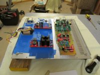
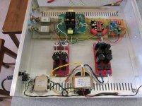
Some progress on the final build. Estimate 30% complete. In case anyone is interested. Big sucker like most of my builds.

On to a winner!
Um, can current stage or CFB stage be put into 'saturation' like a tube?
Thanks for the explanation on current section too.
Um, can current stage or CFB stage be put into 'saturation' like a tube?
Thanks for the explanation on current section too.
Last edited:
Saturation
In my experience, yes. If I understand your question. I have another dac in prototype form it is a parallel TDA1541A S1 Crown dac. WM8804, SM5814, 2 Red Baron boards with S1's. When combining the outputs so it sinks 0-8 mA per channel, it created extreme distortion with every op amp I tried. A resistor I/V worked well in that case. About 25 Ohms was ideal for a parallel dac. With a tube saturation would likely occur with a starved plate situation. A lower then normal B+. ???On to a winner!
Um, can current stage or CFB stage be put into 'saturation' like a tube?
Thanks for the explanation on current section too.
Torchwood421
I think it's better to make it dual differential TDA1541A rather than parrallel. WM8804 is excellent. I also use this receiver chip with TDA1541A and AD844 I/V stage.
I had a parallel TDA1541 DAC but I pulled out one chip and now using single dac with ad844. Parallel is useful for passive i/v. IMHO parallel DAC chip has no advantage when using active I/V stage.
Last edited:
Hi,
I agree and even say that increasing current can be inferior.
Similar to voltage stages the ratio of idle value to ac signal amplitude should be high.
If your stage runs on say 5mA idle current and +-2mA ac signal it'll distort less than running on 2.5mA idle current.
A fine but extreme example is OPCs grounded source MOSFET I/V which idles at up to 70V/500mA iIrc.
The transistor can hardly distinguish between idle and signal mode here.
Hence its THD figures are spectaculary good, probabely even bettering the Datasheet values of the best OPAmp stages.
Its a pity that one can't choose the idle current of the AD844.
In that regard the OPA861 -utilizing the same basic topology- is more flexible, allowing for higher idle currents.
jauu
Calvin
Parallel TDA1541A S1 Crown DAC experiment
Hi quantran, That has always been an option, to go differential. I don't know of a good digital SPDIF splitter inverter. Have a few circuits that are untested (by me) in my archive. Which one is the best? Speed is certainly an issue. Once the PCM1704 build is done my intention is to do some experiments and "tune the S1 crown dac" to my liking. Interesting tidbit.... Find it easier to build a high quality dac around the TDA1541 (no A). It could be a taste thing I suppose.Torchwood421
I think it's better to make it dual differential TDA1541A rather than parrallel. WM8804 is excellent. I also use this receiver chip with TDA1541A and AD844 I/V stage.
I had a parallel TDA1541 DAC but I pulled out one chip and now using single dac with ad844. Parallel is useful for passive i/v. IMHO parallel DAC chip has no advantage when using active I/V stage.
In my experience, yes. If I understand your question ... would likely occur with a starved plate situation. A lower then normal B+.
I meant 'soft clipping' harmonic distortion that arises when tube or tape is over driven, not 'clipping'. Transistors usually clip dependent on design but I wonder if a CFB behaves differently? I can't judge from calvins post, I did not define what type saturation. Even order harmonics...
Impedance crazy - for years I spelled it impendance too!
Impedance is tricky to discern from datasheets, for example I might try OPA2658 in place of a common dual NE opamp, perfect fit, low-Z input, ok current handling (for 1541). BUT the data sheet reads "output stage has been optimized to drive low resistive loads" Does this statement necessarily mean it's high-z output? The 'open loop trans-impedance' of the 2658 is 180kohm. Which I think translates to "you well need a buffer unless your power amp has input impedance of more than this value".
Impedance is confusing, I think, "which device is in charge" with all this see saw matching.
Calvin I couldn't help but notice the 861 ticks all the right boxes for use with TDA1541 as per your earlier (helpful) explanation, but as it's hi-z output, a buffer is required on the output I think. When I see two in series as per AYAII schema I seen, well that makes no sense to me unless buffer is omitted at the end which I doubt.
Last edited:
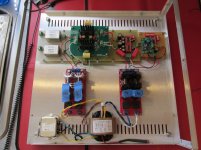
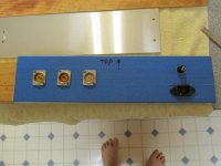
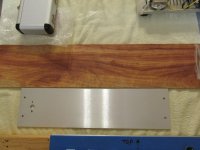
Impedance
I look at impedance as a combination of resistance, capacitance and inductance. My back ground in Amateur radio shapes that I suppose. The trouble is datasheets in general describe the op amp performance in regards to pure resistance and in some cases compensated to drive heavy parallel capacitance loads. Inductance is never mentioned in my experience. The only advice I can give you is to try the more interesting parts in the circuit your trying to tweak. Hands on experimenting pays off in my experience. 861... Never tried it as I moved to the DDNF Pedja discrete circuit. Kind of found nirvana with that. So if you have an interest in the 861 you might want to try it. 🙂 Build progress... Building the back panel. Major holes drilled just need mounting hardware locations drilled.Impedance is tricky to discern from datasheets, for example I might try OPA2658 in place of a common dual NE opamp, perfect fit, low-Z input, ok current handling (for 1541). BUT the data sheet reads "output stage has been optimized to drive low resistive loads" Does this statement necessarily mean it's high-z output? The 'open loop trans-impedance' of the 2658 is 180kohm. Which I think translates to "you well need a buffer unless your power amp has input impedance of more than this value".
Impedance is confusing, I think, "which device is in charge" with all this see saw matching.
Calvin I couldn't help but notice the 861 ticks all the right boxes for use with TDA1541 as per your earlier (helpful) explanation, but as it's hi-z output, a buffer is required on the output I think. When I see two in series as per AYAII schema I seen, well that makes no sense to me unless buffer is omitted at the end which I doubt.
Attachments
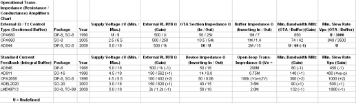
Here's a Tz-Amp spreadsheet which should prove useful for DAC matching, if anyone spots discrepancies on it please feel free to correct it. It's an Microsoft .xls attached in the ZIP. The top three OTAs were tricky to define.
Hopefully I am right in thinking they are the same basic topology with External |Q control.
Hopefully I am right in thinking they are the same basic topology with External |Q control.
Attachments
Nice...
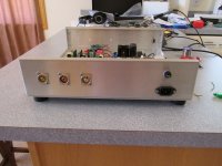
I always liked the sound of the AD846. Sadly it was only 12 bit accurate and obsolete today. AD811... I have used that as an I/V and didn't really like it. Worked great as a buffer amplifier on a DDS (direct digital synthesis) VFO in my other hobby. A RF amplifier in that case. LME49713... Have a few of those. Don't recall much about that. Nothing negative at any rate. Might be worth another listen actually. New build... Sounds better then in prototype form. I then remember I replaced all the Chinese branded electrolytic capacitors with Nichicon's just before getting it in an enclosure. Rule one... Don't use Chinese branded electrolytic capacitors on high quality builds. 😱Here's a Tz-Amp spreadsheet which should prove useful for DAC matching, if anyone spots discrepancies on it please feel free to correct it. It's an Microsoft .xls attached in the ZIP. The top three OTAs were tricky to define.
Hopefully I am right in thinking they are the same basic topology with External |Q control.
- Home
- Source & Line
- Digital Line Level
- Using the AD844 as an I/V