Don't use force, use bigger hammer
HAMs of Yore used 6L6 thrown in bucket of oil, but they did use new one every night
HAMs of Yore used 6L6 thrown in bucket of oil, but they did use new one every night
I'm almost ready to give up. I have a couple things to verify but I can confirm that heatsink is around 30 Degrees C when the fault occurs. It is not heat related.Maybe they are running too hot – almost 40W for a package that is designed for decawatt use.
After failure – did Drain become open circuit?
BTW VGS breakdown is in the 12 to 14V range (in DS).
EDIT: Exactly, as Nelson said ^ it is tiny device (we posted at the same time).
As nelson states, I want to verify vDS of both fets before failure and then I put baby to bed and build the F3. I will put the all parts out to the sidewalk for the next poor bastard. It's been a great learning experience and I can barely get 1W into 8 ohm but its better into 4 ohm.
Sorry, which circuit are you referring to?I agree that changing to the mu/2 circuit should work also, since the output C
will not be connected directly to the upper source.
I question the fact it is not heat related: What's the junction temperature? What's thermal resistance junction to heatsink times 40W, where junction to heatsink is aggregation of at least three values.
Can you measure failed devices and say what's wrong with them, as rayma asked? Please don't give up, maybe you are just too fearless… 🔥
Can you measure failed devices and say what's wrong with them, as rayma asked? Please don't give up, maybe you are just too fearless… 🔥
I'm almost ready to give up. I have a couple things to verify but I can confirm that heatsink is around 30 Degrees C when the fault occurs. It is not heat related.

Yours.Sorry, which circuit are you referring to?
But with the coupling capacitor connected to the lower drain, instead of the upper source.
With tubes (and no loop feedback), that gives a voltage gain of mu/2 when buffered.
https://www.tubecad.com/2005/July/blog0051.htm
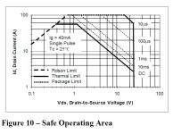
The LU1014D spec sheet gives the Power Dissipation at 25 degrees C as 69W. At operating temperature the maximum dissipation would be much lower. The junction temperature would also be much higher than the 30 degrees at the heat sink.
So if the device was at 40W when it failed, I would say that it was most likely due to excessive power across the device.
Here is the SOA @ 25C from the LU1014D spec sheet:
So if the device was at 40W when it failed, I would say that it was most likely due to excessive power across the device.
Here is the SOA @ 25C from the LU1014D spec sheet:
Attachments
Just wondering here could one replace the upper half (ie. SRPP aka SEPP aka mu-follower, or whatever people call it..) with perhaps something like an IRFP240 instead of LU1014D without losing too much of the sound signature as I assume it's the use of a JFET in the lower half side that sets most of the character, no?
However, as a device like the IRFP VFET's is an enhancement mode device it would need a bit different biasing scheme though.
However, as a device like the IRFP VFET's is an enhancement mode device it would need a bit different biasing scheme though.
I question the fact it is not heat related: What's the junction temperature? What's thermal resistance junction to heatsink times 40W, where junction to heatsink is aggregation of at least three values.
Can you measure failed devices and say what's wrong with them, as rayma asked? Please don't give up, maybe you are just too fearless…
Obv, can't measure the junction temperature but I measure the package temperature with IR gun which is soldered to RF shielding then C-clamped to 100w copper heatsink with a fan on it the package temperature is around 35 degrees C at 20v VCC fault voltage.
I have it running at 18.11vDC drawing 4.3A 77.90W for a couple hours:
Nelson here is vDS values:
Top FET VDS = 9.58vDC
Bottom FET VDS = 4.27vDC
Top source resistor: 1.968vDC
Bottom source resistor: 2.00vDC
Output cap voltage: 8.15vDC
Likely when voltage is brought to 20vDC there is too much voltage on the upper FET (around 12V?) I think that may explain it.
Last edited:
- Home
- Amplifiers
- Pass Labs
- Using LU1014D in parallel for a power amp stage.