Figured out how to open it.
Looks like it is ready to be sent to a PCB maker.
Just a matter of finding one ...
OSHPark for prototype quantities,
Imagineering for productions runs.
nokin,
I tried the 2SK170. It provided almost too much musical energy.
The 2SK246 "Y" and 2SK208 "O" or "R" provide more musical energy and detail than a 6K resistor, but do it in a more balanced and natural way. The 2SK208 is a SOT-23 SMT.
Hi Carlsor,
Can you share us the schematic of this ?
Did anybody here test Pcm1798 on this deck board if it works flawlessly or not ?
I cannot buy Pcm1794 so replaced 2x pcm1798 but it makes hiss noise on output. I can't find out the reason after tried many others testing..
CCS schematic
Nokin,
Go to: http://www.diyaudio.com/forums/digi...ngle-board-pcm1794-nos-dddac.html#post4130328
Nokin,
Go to: http://www.diyaudio.com/forums/digi...ngle-board-pcm1794-nos-dddac.html#post4130328
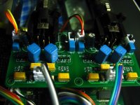
More R2R DAC Buffer Pictures
Attached are two more pictures of the Buffer PCB made by LeonBernieniv for his R2R DAC. Very good looking Buffer job.
The R2R Buffer PCB design is a little different from the first ones used on the DDDAC, but it is still a JFET Buffer with Cascoded JFET CCS at heart. It is dual mono with voltage reference circuits for both sides. All transistors and some capacitors are SMT. The outputs are capacitor coupled. The JFETS are running at 100% Idss with no source resistors or adjustment pot. Some modifications will have to be done to duplicate the circuit function of the DDDAC Buffer. I will need to take a closer look to make sure I totally understand the R2R Buffer layout.
I need the PCB board dimensions and mounting hole distances to see how it might fit on the DDDAC.
Attachments
carlsor, the board had no more changes with circuit even element value but replace ztx450 with bc847, the circuit has a wide swings that I have not changed your bias settings. So I think it can be used directly on here. Notes TL431 is normal pinning(1.cathode, 2.ref, 3.anode)
R2R Buffer Questions
LeonBernieniv,
Thank you again for the use your Buffer pcb design. I have questions to help me understand your circuit layout better.
1. I don't see any resistors to the gates of the BF861 or to the base of the BC847 transistors. Are these located on the bottom of the PCB? I discovered that these eliminate the possibility of transistor oscillation.
2. I don't see a 10 ohm resistor or adjusting 20 ohm pot from the bottom BF861 to -12V. These cause the JFETS to run at 70-80% of their Idss and to reduce the differential output offset to near 0.0mv. We want to drive output transformers, not output coupling capacitors.
3. Why did you use the BF861 instead of the BF862 JFET transistors?
4. What are the dimensions of your PCB and the distances between mounting holes?
5. Who manufactured your board?
Thank You....carlsor
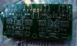
Yes, the resistors was on the bottom side. BF861 is just a name of the lbr I made it. And dim. is about 8x6cm, I'll have a look late. Maybe it should be more mod as you sad. I'm a l33t and just for fun for this.
2SK246Y on eBay
I ordered some . Still available on eBay if you don't want to play with smd like me 😀
I ordered some . Still available on eBay if you don't want to play with smd like me 😀
faint... I'm noooot a l33tYes, the resistors was on the bottom side. BF861 is just a name of the lbr I made it. And dim. is about 8x6cm, I'll have a look late. Maybe it should be more mod as you sad. I'm a l33t and just for fun for this.
Carlsor, the dimensions is 4 inch * 2 inch, distances of holes is 3.7 inch * 1.7 inch.
I know most people do not like SMD, the board seems to be some tendency to personalize, and I also did some "wacky" setting, as you can see the OP-like footprints, but v-cut prices more expensive, then put this grotesque stay on the board, the OP-like also has a separate brd file attached.
So if you really do not like SMD, may need to re-design, there are many real master here, I'll not participate.
Regards
Attachments
R2R Buffer
LeonBernieniv,
As long as the files are masters we can modify as needed. We may have to make a couple of prototype boards to see exactly what you have designed.
I still cannot see how the little "OP-like" board works with the main buffer board.
LeonBernieniv,
As long as the files are masters we can modify as needed. We may have to make a couple of prototype boards to see exactly what you have designed.
I still cannot see how the little "OP-like" board works with the main buffer board.
Carlsor,
I tried to answer your email but it came back as undeliverable. Very strange.
I do not know anyone who I could ask to do pcb design. I would guess we will have to pay someone to make the modifications.
First time I have ever had something interesting in a POP UP ad:
EXTREME Copper Printed Circuit Boards - High Tech PCB Capabilities
Never have seen anything like that. Not that I think it would be good for our purposes but nice to know such a thing is available.
I will keep looking.
Carlsor,
Regarding the CCS implementation on pin 20, is it worthwhile to make an effort to use the trimpot and get the the exact fixed resistor values for each of the CCS after determining those values for the right current or it will be sufficient just to use the same value for all the CCSes? I have a 4 deck so it would be quite some work to do for all of them.
Thanks!
Carlsor,
Regarding the CCS implementation on pin 20, is it worthwhile to make an effort to use the trimpot and get the the exact fixed resistor values for each of the CCS after determining those values for the right current or it will be sufficient just to use the same value for all the CCSes? I have a 4 deck so it would be quite some work to do for all of them.
Thanks!
I have the same issue. My current plan is to calibrate all CCS's individually, record resistor variation, then order correct resister values and put fix values on the CCS's and then put them in the 4board stack and cross fingers. 😉
Keep me posted of your implementation. If the resistor variation isnt big (say less than 5%) I might just use an average of your resistor values. Thanks! 🙂I have the same issue. My current plan is to calibrate all CCS's individually, record resistor variation, then order correct resister values and put fix values on the CCS's and then put them in the 4board stack and cross fingers. 😉
First time I have ever had something interesting in a POP UP ad:
EXTREME Copper Printed Circuit Boards - High Tech PCB Capabilities
Never have seen anything like that. Not that I think it would be good for our purposes but nice to know such a thing is available.
Automotive and other high power applications, been using these and higher weights for many years. You can also use 1oz on outer layers so you can get SMD logic devices for control and have higher weights inside for power transfer. Even done mixed weight copper across a board, 2oz at one end 4oz at the other, very very expensive🙂
The heaviest I have used was 7oz, on some special power distribution fleixis.
Keep me posted of your implementation. If the resistor variation isnt big (say less than 5%) I might just use an average of your resistor values. Thanks! 🙂
I found variation was much greater than 5%, and trying to set the value without being in circuit didn't work. It was dead easy in situ conversely
David
Automotive and other high power applications, been using these and higher weights for many years. You can also use 1oz on outer layers so you can get SMD logic devices for control and have higher weights inside for power transfer. Even done mixed weight copper across a board, 2oz at one end 4oz at the other, very very expensive🙂
The heaviest I have used was 7oz, on some special power distribution fleixis.
That would be quite a PCB at 7 ounces of copper.
THANKS for the information.
A nightmare to soldered, you could burn your hand by the heat transfer across the board. Had to be all preheated correctly then connectors soldered in (no thermal relief either).
Its the ECUs etc on cars, especially high performance ignition systems where you want to move a lot of current and have control.
Its the ECUs etc on cars, especially high performance ignition systems where you want to move a lot of current and have control.
....
Thanks Carlsor..
This is the spread I'm getting for the 2SK208 (with three rejects), 0.400 mA. Middleground gives about 5% fluctuation in the worsts case and tempco for 24-50Celcius is about 1%. Which is all excellent.
I might make another batch to get the spread even closer.
An externally hosted image should be here but it was not working when we last tested it.
Last edited:
I found variation was much greater than 5%, and trying to set the value without being in circuit didn't work. It was dead easy in situ conversely
David
Why wasn't it possible to set the value upfront, I've tried up to 5Vdc fluctuation and the CCS stays dead accurate.., what was different in Situ?
Adjusting in situ is not so easy with multiple dac boards.
- Home
- Source & Line
- Digital Line Level
- Upgraded Single Board PCM1794 NOS DDDAC