LDR Cinemag resistor load
SimonJ
Ed is right - The breadboard contains a pair of LDR resistors in series providing 11K ohms of load resistance to the Cinemags. My preamp input is 330K ohms which makes the Cinemags sound unacceptably bright. A load of 8-15K makes the Cinemags sound right.
The LDRs are powered by the 5V to the WaveIO and can be switched off when connecting the DDDAC to a preamp with 10K input resistance. IMO LDR resistors have a sq that is comparable to the very best fixed resistors. My preamp is a unity gain buffered LDR volume attenuator.
Thanks but LDR can be light dependent resistor so its not that right?
SMD workflow? Sometimes I forget about things like google and youtube myself. And I guess other people do too 🙂 There are plenty of videos on youtube about smd soldering and afterwards cleaning of the parts. Better watch than read.
Thanks but LDR can be light dependent resistor so its not that right? - SimonJ
These are light dependent resistors - two pair.
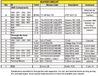
Buffer Board Assembly Instructions
The larger number written on each BF862 pouch is the Idss current. The smaller number is the ma current with a 10ohm source resistor which is the primary number used for matching. Above each pouch is the “Qxx” location on the Buffer Board to install each BF862. The paper pouch is easily opened with a razor blade or X-acto knife. Clean board with isopropyl alcohol before starting.
1. First solder all the BF862’s in their proper location. SMD tweezers are a must! Use the SMD technique of your choice. NOTE: I used a small soldering tip with Wonder solder. The soldering pencil heat was the same as for soldering through-the-hole components. I put a small amount of solder on the gate pad for the JFET. Next I held each BF862 in place and touched the hot tip to the pad leg junction until the solder melted – usually within 1 second. Next I soldered the other leads/ends by putting the solder between the component and the hot tip and pushed through the solder until there was solder flow – again usually no more than 1 sec. You may want to resolder the gate solder joints if they don't look good enough. Next time I am going to first apply a sticky flux to each pad from a syringe applicator to get better solder flow.
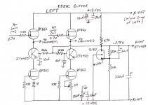
2. TEST: Put your meter in the diode test mode. I will refer to the “IN” and “OUT” sides of the board. Also Q54, Q55, Q64, and Q65 will be referred to as ZTX450 transistors with the TO-92 hole-pads used for test measurements. The BF862’s and their solder connections can be tested by putting the red/pos probe on the JFET gate and touching the black meter lead to each end of the BF862 circuitry as follows:
- Measure the four IN side BF862’s from gate to +12V (OUT side) and then to the ZTX450 IN side hole-pads for each BF862. The 8 readings should be very similar.
- Next measure the four OUT side BF862’s from gate to the ZTX450 OUT side hole-pads for each BF862 and then to the 10 ohm resistor or pot connected to each of these BF862’s. Again you should get 8 similar reading.
- If you measure a short or no connection then there is a soldering or component problem to fix. All my BF862 diode test readings were around 0.7 on my Fluke 77.
- If this is too confusing then just measure from the BF862 gates to both end legs on the BF862 transistors. A hand drawn circuit is provided to help with testing and troubleshooting.
3. Next install all of the SMD resistors. The BOM picture shows which resistor value goes in each location.
4. TEST: Put meter in ohms-resistance mode.
- Measure from +12V to -12V. This should read 41.7K.
- Measure from the C52 + square hole to the middle hole-pad of each ZTX450 – you should get four readings of 240 ohms.
- Measure from the gates of the IN BF862’s to the IN +R, -R, +L, and –L points that they are connected to. You should read 470 ohms.
- Measure the ohms from the gates of the OUT BF862’s to the -12V (OUT side). They should all read 470 ohms.
5. Next install all through-the-hole transistors, capacitors, terminal blocks and 20 ohm pots. Make sure that the center lead of the pots read close to 10ohms from each end before installing them.
6. TEST: Put meter in ohms-resistance mode.
- Measure from IN +R to –R and from +L to –L. You should get >10 Meg ohms or open circuit. Next measure from each of these points to GND. You should get 0.5-2 Meg ohms. Getting similar measurements for the left and right sides is more important than getting these estimated values.
- Measure from +12V to -12V. The reading should soon be greater than 10K ohms and rising because of the charging of the caps. A short reading would be bad here.
- Measure R+ OUT to R- OUT and L+ OUT to L- OUT. You should get between 25 and 70 ohms. Getting similar measurements for the left and right sides is more important here.
7. Connect the Buffer board as follows:
- Power supply to +12V, -12V, and GND. This power supply ground should be connected to the 8V analog power supply ground.
- Connect Right Main Board Pos to R+IN, Right Main Board neg to R-IN and Left Main Board Pos to L+IN, Left Main Board neg to L-IN.
- Do NOT connect anything to the OUT terminals at this time!
7. Physically mount the Buffer board to the Main Board or DAC board. See pictures at http://www.diyaudio.com/forums/digit...ml#post4230292
8. Power up the DAC and Buffer Board assembly.
9. TEST: Meter in Volts mode:
- Verify +12 and -12V on buffer board relative to DAC board ground.
- Measure from GND to R53 on far left which should be about -2.8V. This verifies the constant voltage circuit.
- The 4 IN points should be around 2.7V, and most importantly, within 0.01V of each other for each differential pair.
- The 4 buffer OUT points should measure about 0.1V higher than the IN points at around 2.8V.
10. Buffer Pot adjustment: (If only single ended capacitor output is to be used, then skip this step.) Put meter in MV measurement mode and put leads across R+ and R- Buffer OUT. Adjust pot to get close to 0.0mv. Do the same for L+ and L- OUT. Wait at least 30 minutes for the DAC to heat up and repeat adjustment. Turn off power.
11. Connect Cinemag, other output transformer, or differential capacitor leads to R+ and R- Buffer OUT and L+ and L- OUT. Turn on Power and check voltage across OUT leads. If ok then start listening to music.
The larger number written on each BF862 pouch is the Idss current. The smaller number is the ma current with a 10ohm source resistor which is the primary number used for matching. Above each pouch is the “Qxx” location on the Buffer Board to install each BF862. The paper pouch is easily opened with a razor blade or X-acto knife. Clean board with isopropyl alcohol before starting.
1. First solder all the BF862’s in their proper location. SMD tweezers are a must! Use the SMD technique of your choice. NOTE: I used a small soldering tip with Wonder solder. The soldering pencil heat was the same as for soldering through-the-hole components. I put a small amount of solder on the gate pad for the JFET. Next I held each BF862 in place and touched the hot tip to the pad leg junction until the solder melted – usually within 1 second. Next I soldered the other leads/ends by putting the solder between the component and the hot tip and pushed through the solder until there was solder flow – again usually no more than 1 sec. You may want to resolder the gate solder joints if they don't look good enough. Next time I am going to first apply a sticky flux to each pad from a syringe applicator to get better solder flow.
2. TEST: Put your meter in the diode test mode. I will refer to the “IN” and “OUT” sides of the board. Also Q54, Q55, Q64, and Q65 will be referred to as ZTX450 transistors with the TO-92 hole-pads used for test measurements. The BF862’s and their solder connections can be tested by putting the red/pos probe on the JFET gate and touching the black meter lead to each end of the BF862 circuitry as follows:
- Measure the four IN side BF862’s from gate to +12V (OUT side) and then to the ZTX450 IN side hole-pads for each BF862. The 8 readings should be very similar.
- Next measure the four OUT side BF862’s from gate to the ZTX450 OUT side hole-pads for each BF862 and then to the 10 ohm resistor or pot connected to each of these BF862’s. Again you should get 8 similar reading.
- If you measure a short or no connection then there is a soldering or component problem to fix. All my BF862 diode test readings were around 0.7 on my Fluke 77.
- If this is too confusing then just measure from the BF862 gates to both end legs on the BF862 transistors. A hand drawn circuit is provided to help with testing and troubleshooting.
3. Next install all of the SMD resistors. The BOM picture shows which resistor value goes in each location.
4. TEST: Put meter in ohms-resistance mode.
- Measure from +12V to -12V. This should read 41.7K.
- Measure from the C52 + square hole to the middle hole-pad of each ZTX450 – you should get four readings of 240 ohms.
- Measure from the gates of the IN BF862’s to the IN +R, -R, +L, and –L points that they are connected to. You should read 470 ohms.
- Measure the ohms from the gates of the OUT BF862’s to the -12V (OUT side). They should all read 470 ohms.
5. Next install all through-the-hole transistors, capacitors, terminal blocks and 20 ohm pots. Make sure that the center lead of the pots read close to 10ohms from each end before installing them.
6. TEST: Put meter in ohms-resistance mode.
- Measure from IN +R to –R and from +L to –L. You should get >10 Meg ohms or open circuit. Next measure from each of these points to GND. You should get 0.5-2 Meg ohms. Getting similar measurements for the left and right sides is more important than getting these estimated values.
- Measure from +12V to -12V. The reading should soon be greater than 10K ohms and rising because of the charging of the caps. A short reading would be bad here.
- Measure R+ OUT to R- OUT and L+ OUT to L- OUT. You should get between 25 and 70 ohms. Getting similar measurements for the left and right sides is more important here.
7. Connect the Buffer board as follows:
- Power supply to +12V, -12V, and GND. This power supply ground should be connected to the 8V analog power supply ground.
- Connect Right Main Board Pos to R+IN, Right Main Board neg to R-IN and Left Main Board Pos to L+IN, Left Main Board neg to L-IN.
- Do NOT connect anything to the OUT terminals at this time!
7. Physically mount the Buffer board to the Main Board or DAC board. See pictures at http://www.diyaudio.com/forums/digit...ml#post4230292
8. Power up the DAC and Buffer Board assembly.
9. TEST: Meter in Volts mode:
- Verify +12 and -12V on buffer board relative to DAC board ground.
- Measure from GND to R53 on far left which should be about -2.8V. This verifies the constant voltage circuit.
- The 4 IN points should be around 2.7V, and most importantly, within 0.01V of each other for each differential pair.
- The 4 buffer OUT points should measure about 0.1V higher than the IN points at around 2.8V.
10. Buffer Pot adjustment: (If only single ended capacitor output is to be used, then skip this step.) Put meter in MV measurement mode and put leads across R+ and R- Buffer OUT. Adjust pot to get close to 0.0mv. Do the same for L+ and L- OUT. Wait at least 30 minutes for the DAC to heat up and repeat adjustment. Turn off power.
11. Connect Cinemag, other output transformer, or differential capacitor leads to R+ and R- Buffer OUT and L+ and L- OUT. Turn on Power and check voltage across OUT leads. If ok then start listening to music.
Attachments
SimonJ
IMO LDR resistors have a sq that is comparable to the very best fixed resistors.
I had heard that re SQ but also that the problem was getting a matched pair for decent channel balance?
David
Buffer Board Assembly and Burn-in
The assembly and testing instructions I posted are for those who would like confirmation of every step being right. If you are confident in your SMD soldering then solder everything to the board and proceed to step 6. If you don't get the expected measurements then you can go back to earlier steps for trouble shooting.
The burn-in period is not as ugly sounding as I made it out to be. The first 1-2 hours sounded rough but by late evening my DDDAC-Buffer assembly was sounding so good that I was reluctant to leave it to go to bed. I just want to keep you all from making hasty decisions about the sound of the buffer. If you like the sq after a few hours, you will love it after 300 hours.
The buffer, CCS, and upgraded 8V PCM1794 regulated power supply together act like a magnifying glass on everything that is right or deficient in your digital sources and digital voltage regulation. Upgrades in the digital section will more discernible after all the analog upgrades have been made.
Last edited:
Enrico,
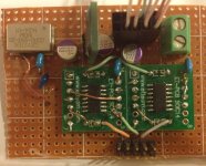
Yes, this is a simple reclocker with just a 100mhz Crystek and two Potato PO74G74A D-flip flop chips. I posted this at http://www.diyaudio.com/forums/digi...pcm1794-waveio-usb-input-346.html#post4120369 including a picture. I think I have a picture of the schematic somewhere if you are interested.
There are no instructions on what components to put on the Acko S03 board to work best with the WaveIO so I am staying with the breadboard for awhile. The change in sq is very small - unlike the CCS boards which result in a big change in the liveliness and detail of sound.
id like to see the reclocker details too
thnx
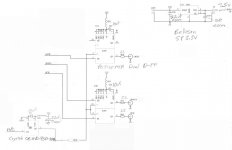
Simple Reclocker Schematic
Attached is a rough schematic of the asynchronous reclocker circuit I built.
I did not install the FB1-3 inductors.
The 10nf caps at C7, C23, and C24 are C0G ceramics.
The circuit uses 70-80ma of 3.3V power. The Crystek clock has an internal output buffer capable of supplying 25ma. One set of the ribbon cable pins are connected to pass 5V power from the DDDAC Main board to the isolation buffer located on the WaveIO board.
This is a nasty breadboard undertaking. The dark blue cap in the picture is not being used. A PCB for this would be much better.
I received permission to do this after I did the breadboard as follows:
"I have checked with Acko and it is alright to share or use the re-clocker circuit and concepts for your projects.
Regards,
Jason"
This circuit ONLY works with the WaveIO and NOT with the rpi, Amanero, or bbb.
Attachments
https://hifiduino.wordpress.com/2012/12/01/amanero-reclocking-352-8k384k/
this the same?
does it mean we could tap into the mck of the pcm1794 instead of using bck?
maybe im just confused
this the same?
does it mean we could tap into the mck of the pcm1794 instead of using bck?
maybe im just confused
This circuit appears the same - this is the first time I have seen this document.this the same? nige2000
I couldn't find any mck on the PCM1794 chip diagram. This DAC chip supposedly creates its own master clock internally from the incoming I2S signals.
I don't understand your question or the meaning of the word "scope" here.Ross, I am confused too... which is the scope to reclock the waveio? emyeuoi
I don't understand your question or the meaning of the word "scope" here.
Sorry... my bad english again.
I mean, why you need to re-clock the Waveio?
As far I understand the Waveio from Doede, that I suppose we are talking about, will play any file from 44.1 to 192 kHz
This circuit appears the same - this is the first time I have seen this document.
I couldn't find any mck on the PCM1794 chip diagram. This DAC chip supposedly creates its own master clock internally from the incoming I2S signals.
.
Sorry it's labeled sck system clock
dddac has it merged in to bck
just wondered if since you have the clock signal could it be used or used to any benefit?
suppose we need to ask deode
Why a Reclocker on WaveIO?
Someone reported that a reclocker made an improvement in sq from the WaveIO. Because I had done every other upgrade I could think of I built a reclocker with just the D-FF chips, a low jitter clock, and continued to use the isolator located on the WaveIO chip. The Crystek is a better quality clock than the one on the WaveIO.
This reclocker does not create any new clock signals - it just cleans up the I2S bits stream from the WaveIO regardless of the file bit rate. The improvement in sq is just a hair above imaginary. I recommend that all other upgrades be done first including better voltage regulation on the digital circuits and on the WaveIO.
didn't find much info on sck
anyone know anything?
my experience with clocks is that there extremely extremely sensitive to power supply
no matter what the sales spiel is
id prioritise the ps for the clock before the clock itself
which clocks is on the waveio btw?
anyone know anything?
my experience with clocks is that there extremely extremely sensitive to power supply
no matter what the sales spiel is
id prioritise the ps for the clock before the clock itself
which clocks is on the waveio btw?
Clock Power Supplies
I agree. That's why I have a Belleson SP on the simpler reclocker and Belleson SPM's on the digital side of the PCM1794 chips which are also functioning internally as a clock.
I am in the final stages of making local digital voltage regulators based on the ADM7150 linear voltage regulator. The diyinhk power supplies and the highly regarded Pulsar clock use this regulator chip. The parts for three ADM7150 voltage regulators costs about the same as for one Belleson or Tent Labs regulator. I will post pictures and listening impressions when I am done.
my experience with clocks is that there extremely extremely sensitive to power supply - nige2000
I agree. That's why I have a Belleson SP on the simpler reclocker and Belleson SPM's on the digital side of the PCM1794 chips which are also functioning internally as a clock.
I am in the final stages of making local digital voltage regulators based on the ADM7150 linear voltage regulator. The diyinhk power supplies and the highly regarded Pulsar clock use this regulator chip. The parts for three ADM7150 voltage regulators costs about the same as for one Belleson or Tent Labs regulator. I will post pictures and listening impressions when I am done.
I'm interested in your reclocker, in fact behind an i2s switch between waveio and (isolated) raspberry Pi.This circuit ONLY works with the WaveIO and NOT with the rpi, Amanero, or bbb.
Why is your reclocker not working with rpi?
- Home
- Source & Line
- Digital Line Level
- Upgraded Single Board PCM1794 NOS DDDAC