Структура Ломакин Паршин лишь похожа на Видерхольда,но это совсем иной усилитель с вложенной оос и инверсией входов оу
Maxim, so in your opinion - which one should perform better?
Wiederhold or Lomakin/Parshin?
Both are good.
I don't want to compare them.I like LMK with 4 pairs of outputs.Well, the monster in the new edition
I don't want to compare them.I like LMK with 4 pairs of outputs.Well, the monster in the new edition
Last edited:
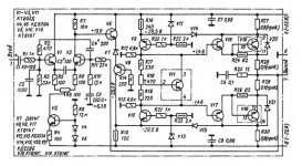
Hope not a silly question, what's the purpose of that grounded base Q2 transistor in post #172 schematic?
regards
JJT
regards
JJT
Hope not a silly question, what's the purpose of that grounded base Q2 transistor in post #172 schematic?
regards
JJT
This is a voltage level shift cascade
From the original German article:
The transistor Q2 plays the role of servo voltage follower,
working with a common base,
matches the low output impedance of the Q1 buffer, with a two-stage current amplifier.
With this construction of the amplifier, it becomes possible
get output amplitude signal at load close
to the supply voltage (rails) - instead of the rail voltage of an operational amplifier, with minimal distortion of form.
This is a voltage level shift cascade
cascade => cascode ?
No, not in this design.
In few weeks I'll publish Wiederhold amp with drivers and all N-channel HexFets (E.g. IRFP240).
Quasi !!
Have it in the works now, seems very promising, and quasi design is more in the spirit of the original 1977 design 🙂.
I see, you mean HEXFET quasi design is similar to the BJT version, I will wait then, I really want to use those HEXFETs, hope it is really similar to the BJT performance.
This common based VAS principle used in Vhex+ amplifier as well (with LTP front end). Vzaichenko named it "current driven VAS" or "current subtraction" approach. VAS output is arranged as two current sources, looking at each other. One of them is driven by the current from the single-ended VAS input transistor in a way, that its current is subtracted from the current, set by the upper CCS's emitter resistor. The structure appears to be extremely linear and stable.
Its benefits are the follows:
- High immunity to external noises, especially EMF-induced ones;
- Low distortion open-loop - i-to-v (transimpedance) stage is highly linear;
- Low phase shifts throughout the whole audio bandwidth, requiring very low compensation for demonstrating high stability margins and resulting in very good - accurate, natural - sound reproduction;
- High enough slew rate by design - "current drive" front-ends easily achieve 150-400V/uS, providing high dynamic characteristics;
- This approach gives high speed, linearity and phase of the open loop circuit, ensuring good stability margins with the global loop closed
Last edited:
It will the icing on the cake. 😉In few weeks I'll publish Wiederhold amp with drivers and all N-channel HexFets (E.g. IRFP240).
Quasi !!
Have it in the works now, seems very promising, and quasi design is more in the spirit of the original 1977 design 🙂.
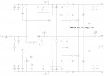
Looks like this (attached).
Everything seems to be based on something 🙂
It retains the same overcurrent protection as used in original Wiederhold quasi design.
Everything seems to be based on something 🙂
It retains the same overcurrent protection as used in original Wiederhold quasi design.
Attachments
Last edited:
Looks like this (attached).
Everything seems to be based on something 🙂
It retains the same overcurrent protection as used in original Wiederhold quasi design.
stolen before us
minor fixes for MOS200
A couple whoops:
1. D1 and D3 are swapped. The Zeners are probably a waste because VtoM1+VtoM2 (ie VQ2) < Vz so just D1 and D2 are needed.
2. R6 needs to be about 12K to balance the LTP and improve THD. Or you could increase R5 and maybe loose R13.
3. D5 is not a great idea unless you add a Zener. Or you could change R7=~7.5K, R8=~1.8K so that the bootstrap is limited to about 10V.
4. R9, R10 are excessive, maybe 220?
5. A diode in series with R16 may reduce turn-off thump.
6. R1,R2,R3,R4 are awkward and overbiased. I recommend loosing R1 and replacing R3,R4 with 1K paralleled with 10K for similar bias or paralleled with 18K for a lower bias.
This is a very quick and simple amp that has lots of room for improvements.
Attached.
A couple whoops:
1. D1 and D3 are swapped. The Zeners are probably a waste because VtoM1+VtoM2 (ie VQ2) < Vz so just D1 and D2 are needed.
2. R6 needs to be about 12K to balance the LTP and improve THD. Or you could increase R5 and maybe loose R13.
3. D5 is not a great idea unless you add a Zener. Or you could change R7=~7.5K, R8=~1.8K so that the bootstrap is limited to about 10V.
4. R9, R10 are excessive, maybe 220?
5. A diode in series with R16 may reduce turn-off thump.
6. R1,R2,R3,R4 are awkward and overbiased. I recommend loosing R1 and replacing R3,R4 with 1K paralleled with 10K for similar bias or paralleled with 18K for a lower bias.
This is a very quick and simple amp that has lots of room for improvements.
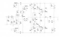
Wiederhold77 HexFet Quasi
Here is the HexFet Quasi version that I'm building next.
For some strange reason, it sims better than LatFet version, which I guess can't be true.
So my guess is it's gonna be good enough.
I have whole bucket of N channel fets (FQA28N15) to use..
Here is the HexFet Quasi version that I'm building next.
For some strange reason, it sims better than LatFet version, which I guess can't be true.
So my guess is it's gonna be good enough.
I have whole bucket of N channel fets (FQA28N15) to use..
Attachments
- Home
- Amplifiers
- Solid State
- Unusual amp from 1987