I have tried with source resistors of 0.22 Ohms in my setup today and the thermal runaway with the verticals was gone.
The BJT for bias compensation was still in place, no overcompensation at all, @AKSA. In this setup, the bias stayed at 130mA as I had set it, without signal and after running 500mV input for a while and then letting it rest again.
My board was not planned with room for source resistors, so I cut the source pin and soldered the resistor in for the test.
😵 without heatsink?running 500mV input for a while

Of course not 😀. The above pic is just to show how I added the resistors. Afterwards I mounted the board on the heatsink again.without heatsink?
I never got any clear answers to why Pass F4 can use TL431 for bias control, while this amp supposedly can't. Is it because the F4 runs on a highe quiescent current? If thats the case, I guess I can do the same with my amp?
Pass F4:

Ultra HEXFET:

Time will show, because I am (very) slowly progressing with my project:

🙂 morten
Pass F4:
Ultra HEXFET:
Time will show, because I am (very) slowly progressing with my project:
🙂 morten
TL431 could be noisy if used in the front stage.I never got any clear answers to why Pass F4 can use TL431 for bias control, while this amp supposedly can't. Is it because the F4 runs on a highe quiescent current? If thats the case, I guess I can do the same with my amp?
The Vbe multiplier position is at the output stage. It seems to be fine for me. As it is not possible to thermal couple with TL431, you need a big heat sink.
You are limited by the voltage rating of the JFET, paralleling 2 mosfets is overkill.
Thanks jxdking! Yes, I am aware of the voltage limitation, so I will try something like +/- 20V...24V suooly.
And I like overkill when it is cheap AND easy! 😎
And I like overkill when it is cheap AND easy! 😎
Hello, I am new to the forum.
I would like to upgrade my amplifier nad c316bee . An engineer advised me to changing the input buffer transistors from NPN to a
J-Fet (J112 or 2SK246). Is there a noticeable difference? Where is it located on the board?

I would like to upgrade my amplifier nad c316bee . An engineer advised me to changing the input buffer transistors from NPN to a
J-Fet (J112 or 2SK246). Is there a noticeable difference? Where is it located on the board?
Attachments
Hi omair,
I suggest posting this under a thread for the nad c316bee or starting a new thread. Discussing it here is off-topic for this thread.
This thread might be a good place to start looking: NAD C316BEE - V2 version ( schematics ? )
I suggest posting this under a thread for the nad c316bee or starting a new thread. Discussing it here is off-topic for this thread.
This thread might be a good place to start looking: NAD C316BEE - V2 version ( schematics ? )
Last edited:
Yes, I tried, but I didn't get an answer in the same topic. I saw that you are discussing a transistor J-Fet J112here.
I am very sorry
I am very sorry
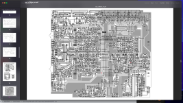
and you want to replace Q101 then simply dropping in a JFET would cause a bias shift that needs correcting. Diodes D101 and D102, Resistors R121 and R119 exist to bias an NPN transistor and would have to be altered, possibly to a ground connection. A JFET would cause an DC offset at C115 that may work with some loss of headroom. It's a bit like saying that you can replace a horse with a camel. Yes and No.Hello, I am new to the forum.
I would like to upgrade my amplifier nad c316bee . An engineer advised me to changing the input buffer transistors from NPN to a
J-Fet (J112 or 2SK246). Is there a noticeable difference? Where is it located on the board?
Nobody is answering because your question is based on poor information. I could just say that you cannot simply replace a NPN with a JFET, but there is a possibility that it could be done if you modify other parts in the circuit. If this is the circuit
I am very interested in some 2SJ109V, maybe also some 2SK389V.I have plenty of 2SJ109-2SK389, GR-BL and V versions. PM if interested.
R
Unfortunately I can't write a PM.
Maybe because I am new here.
May I ask you to contact me.
Thanks a lot! 8o)
- Home
- Amplifiers
- Solid State
- Ultra Amplifier with JFET input and Lateral MOSFET out