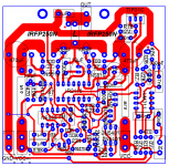
I make PCB from NMOS schematic. Its small (7,2 x 7.5cm). On board i dont have input limiter and DC protection becase I have it. Output filter will have a little long "legs" (1.5cm) for conection with the board.
Attachments
About short curcuit protection and over load protection with NE555 and optocoupler, for other supplay voltage is important voltage drop on 0.1 ohm resistor on main positiv supplay rail.
In original schematic, autor say: +-80V 4 ohms load, around 800W of output power and we need power supplay of 20A (2x10A on positiv and negativ reil).
- On example, 10A shall be our limit.
With 10A curent, resistor of 0.1ohm will have 1V voltage drop. and this is now inportant.
-So, to have the same voltage drop on +-60V (limt is +-57V) we need higher resistance of 0,1 ohm.
So autor say +-57V 14.3A on 4 ohms load.
14.3A / 2 = 7.15A
R= 1V / 7,15A = 0.139 ohms. It means 2 resistor of 0.27 ohms in parallel.
Is this corect?
Thank you
About short curcuit protection and over load protection with NE555 and optocoupler, for other supplay voltage is important voltage drop on 0.1 ohm resistor on main positiv supplay rail.
In original schematic, autor say: +-80V 4 ohms load, around 800W of output power and we need power supplay of 20A (2x10A on positiv and negativ reil).
- On example, 10A shall be our limit.
With 10A curent, resistor of 0.1ohm will have 1V voltage drop. and this is now inportant.
-So, to have the same voltage drop on +-60V (limt is +-57V) we need higher resistance of 0,1 ohm.
So autor say +-57V 14.3A on 4 ohms load.
14.3A / 2 = 7.15A
R= 1V / 7,15A = 0.139 ohms. It means 2 resistor of 0.27 ohms in parallel.
Is this corect?
Thank you
I think yes but not tested, have fineshed latest PCB in next Thread check it
Last edited:
Voxac30:
The original schematic has some I'd say errors. (it works, but not too good performance)
An externally hosted image should be here but it was not working when we last tested it.
Dzony: i killed noise to a minimal level. I had clues about noise, from your post i got sure. I increased 100p to 1n, and decreased 47k to 22k at input. If all the inputs are open, then there is almost audable hiss (with a horn loaded cab..., with 0,1W output you cannot hear noise 😀)
Have check original schematic amd yours, there are differences in LM311 wires
1. LM311 PIN 5,6,7,8 in original schematic from Author goes to +3 V
In your design Pin 7 goes via 470 R to -15V, I think this is wrong
please checkit or can it be there is failure in my design and authors ?
Attachment latest UCD PCB 157 * 80 mm, looks small and nice now....
and have remove 1uf cab from coil to negative rail
...dont like firework after first test PCB
Attachments
NMOS: I have some doubths about this protection. Of course it can work, but:
- The shunt is before caps. The energy stored in caps can be enough, if theres a quick short on output, to kill them, before overcurrent trips.
- 0,1 Ohm shunts are pretty high. Its against the conpect of class-D. The disspiation in this shunt will be higher, than in the IRFP250Ns.
- It still only senses one side.
- Why an NE555? The optocouiple could set SD pin of IR2110 to high, turning it off.
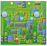
Look at Dzony's PCB design. On first look it looks much better. Your PCB still looks like Class-B stuff. You need a concept change.
I don't like limiters. In my opinion, they do more harm than good.
- The shunt is before caps. The energy stored in caps can be enough, if theres a quick short on output, to kill them, before overcurrent trips.
- 0,1 Ohm shunts are pretty high. Its against the conpect of class-D. The disspiation in this shunt will be higher, than in the IRFP250Ns.
- It still only senses one side.
- Why an NE555? The optocouiple could set SD pin of IR2110 to high, turning it off.
Look at Dzony's PCB design. On first look it looks much better. Your PCB still looks like Class-B stuff. You need a concept change.
I don't like limiters. In my opinion, they do more harm than good.
NMOS: I have some doubths about this protection. Of course it can work, but:
- The shunt is before caps. The energy stored in caps can be enough, if theres a quick short on output, to kill them, before overcurrent trips.
- 0,1 Ohm shunts are pretty high. Its against the conpect of class-D. The disspiation in this shunt will be higher, than in the IRFP250Ns.
- It still only senses one side.
- Why an NE555? The optocouiple could set SD pin of IR2110 to high, turning it off.
Look at Dzony's PCB design. On first look it looks much better. Your PCB still looks like Class-B stuff. You need a concept change.
I don't like limiters. In my opinion, they do more harm than good.
> 0,1 Ohm shunts are pretty high.
ok which value would you recommend for +/- 85V DC Rail, have +/- 85V DC SMPS from defectice PA Amp
> Why an NE555? The optocouiple could set SD pin of IR2110 to high, turning it off.
In like improvement, but its first time for me with Class D
can you provide schematic how to turning off SD pin in overcurrent situation ?
do you have working circuit for overcurrent situation to adapt ?
have found circuit for UCD Bridge Amp with LM311 Protection and only Shunt senses one side too, is this better protection compare to NE555 with opto coupler
Attachments
Last edited:
Guys, I'd really recommend to redo the layout with double sided PCB with proper grounding.
Also the basic current loops on the PCB are far from optimum.
There's a good reason for IR2110 to have 2 "ground" connections, take advantage of that.
Why waste so much effort you've had here with sub optimum layout anyway?
Also the basic current loops on the PCB are far from optimum.
There's a good reason for IR2110 to have 2 "ground" connections, take advantage of that.
Why waste so much effort you've had here with sub optimum layout anyway?
Guys, I'd really recommend to redo the layout with double sided PCB with proper grounding.
Also the basic current loops on the PCB are far from optimum.
There's a good reason for IR2110 to have 2 "ground" connections, take advantage of that.
Why waste so much effort you've had here with sub optimum layout anyway?
please give us sample for optimum Class D ayout, have only experience with Class AB
Last edited:
NMOS:
I would not reccomend this protection. An opto needs ~1,5V to turn on. So resistor value is: R=1,5V/Itrip (the overcurrent treshold), losses are P=1,5/Itrip*I^2. The way it is put can be more simple (the transitor of the opto connects SD to IR2110 supply, with a pull-down resistor to Vn), and more effective (put it after the caps, both lines), just think a bit. A change from an opto to a transitor (0,7V turn on), halfs the losses. Using comparators (treshold voltages can be much less), cuts the losses to minimal.
Why would you choose class d with minimal losses, when the losses of every other part in the schematics (TIP31, making +-3V from +-85V, shunt...) is much greater than the losses from the main FETs.
There are lot of samples, just read AN-1135 "PCB Layout with IR Class D Audio Gate Drivers", AN-1138... Mine needs lot of improvements too (I still have a lot to learn), but the problem with your design, NMOS, is that you still design it as a Class-B amp. Dzony did much better with even a one-sided board. A said lots of times, that if you have double sided PCB, use up ALL the empty space for planes (see AN-1135), and easy heatsinking of the FETS (putting them right to the side of the board) should not be the first priority. With good fets and good design, a simple few-inch Al profile does the job.
I forgot 470 ohm resistor beetwen pin 1 and pin 4 of LM311N
In .zip file you have changed layout with this resistor and pcb.
Conect two stars with short wire like "big" jumepr (this is your feedback)
Check board one more time before, if you find any error, tell me how I can fix it.
If anyone use PCB Wizard, I can send original .pcb file
Regards
In .zip file you have changed layout with this resistor and pcb.
Conect two stars with short wire like "big" jumepr (this is your feedback)
Check board one more time before, if you find any error, tell me how I can fix it.
If anyone use PCB Wizard, I can send original .pcb file
Regards
Attachments
A good PCB comes from understanding some basic principles.
A short remainder:
1. Current always flows in loops (kirhchoff's law)
2. Inductance of the loop is mainly dependant of the geometric area. You may understand a loop as a single turn solenoid, a big loop has pretty some inductance and open flux, I mean it becomes an antenna
3. If return current flows through a bottom layer plane, it flows directly under the signal on the top layer trace because of proximity effect. Therefore current loops related to bottom layer plane have minimum areas and all the inductances are reduced to absolute minimum.
4. Why we want to reduce inductance is because it creates resonant circuits with capacitances. When you get a resonance the way to kill it is by resistance (manipulating Q factor)
5. 10mm of a trace on FR4 board over a return plane has around 10nH.
6. TO220 mosfets have internal inductances of around 5 to 8nH, TO247 are much worse.
7. Control loops (gate driving) must be traced separate from power loops, whch exhibit high di/dt.
8. SMD parts have much lower inductances, this is ecpecially important for capacitors.
A good PCB comes from understanding some basic principles.
A short remainder:
1. Current always flows in loops (kirhchoff's law)
2. Inductance of the loop is mainly dependant of the geometric area. You may understand a loop as a single turn solenoid, a big loop has pretty some inductance and open flux, I mean it becomes an antenna
3. If return current flows through a bottom layer plane, it flows directly under the signal on the top layer trace because of proximity effect. Therefore current loops related to bottom layer plane have minimum areas and all the inductances are reduced to absolute minimum.
4. Why we want to reduce inductance is because it creates resonant circuits with capacitances. When you get a resonance the way to kill it is by resistance (manipulating Q factor)
5. 10mm of a trace on FR4 board over a return plane has around 10nH.
6. TO220 mosfets have internal inductances of around 5 to 8nH, TO247 are much worse.
7. Control loops (gate driving) must be traced separate from power loops, whch exhibit high di/dt.
8. SMD parts have much lower inductances, this is ecpecially important for capacitors.
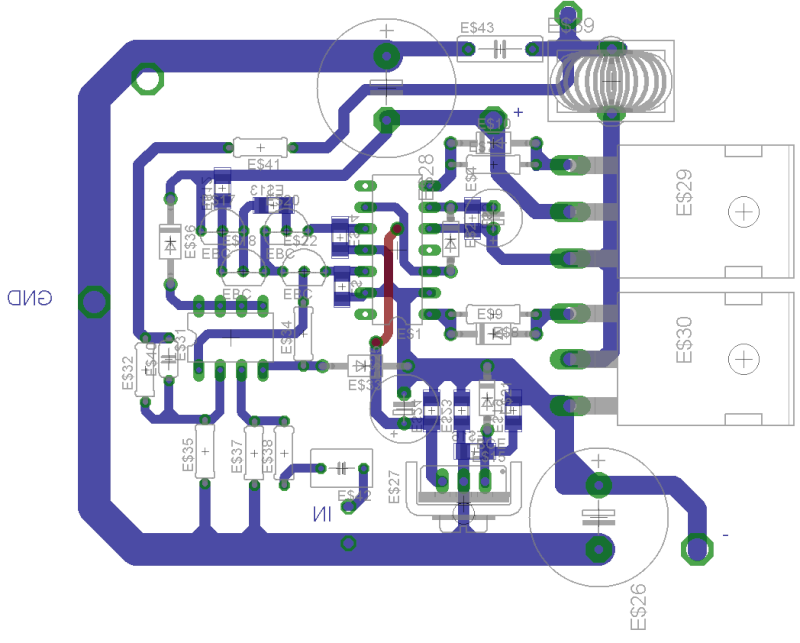
Hello, have redesign PCB, please check it, on TOP Layer have big GND
is it ok now ?
Attachments
A good PCB comes from understanding some basic principles..
Keep tracks short.
Leave as much copper on the pcb as you can especially the ground plane. Not only reduces impedance but saves the planet too.
PCB UCD 25.12.2010.pdf
With this thread being about bringing 25W to 1200kW, it's nice seeing such high activity on the 25/12! 😀
I forgot 470 ohm resistor beetwen pin 1 and pin 4 of LM311N
In .zip file you have changed layout with this resistor and pcb.
Conect two stars with short wire like "big" jumepr (this is your feedback)
Check board one more time before, if you find any error, tell me how I can fix it.
If anyone use PCB Wizard, I can send original .pcb file
Regards
Dzony988: I am using PCB wizard, Please post the pcb file.
Thanks
Raj
Hi !
There are diferences in Schematics -Dzony had diferent supply for LM to original,-Dzony your amp is working can you send a parts list and schematic of your PS?. I think I will use your PCB for first project to learn how work such class d amp
Thanks
There are diferences in Schematics -Dzony had diferent supply for LM to original,-Dzony your amp is working can you send a parts list and schematic of your PS?. I think I will use your PCB for first project to learn how work such class d amp
Thanks
With this thread being about bringing 25W to 1200kW, it's nice seeing such high activity on the 25/12! 😀
very cold, SNOW and ICE Storm outside, its better stay home and design PCB in this cold winter days...and enjoy sound in summer
- Home
- Amplifiers
- Class D
- UCD 25 watts to 1200 watts using 2 mosfets