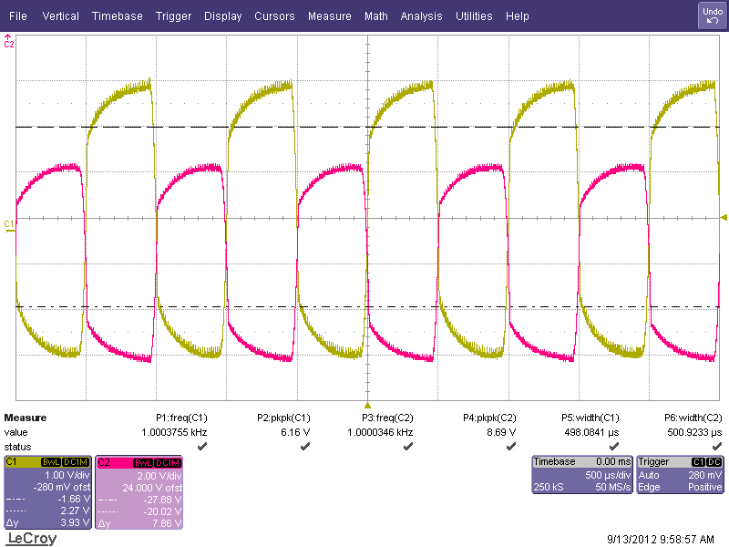
guys, anyway suggestion to improve the irs900d performance? i've used the original irs900d with some extra caps bypass but still sticking to the original tl071, cd4049, ir2110 but with irfb5615 and 20uh i got these at the output:
at the mosfet gate:
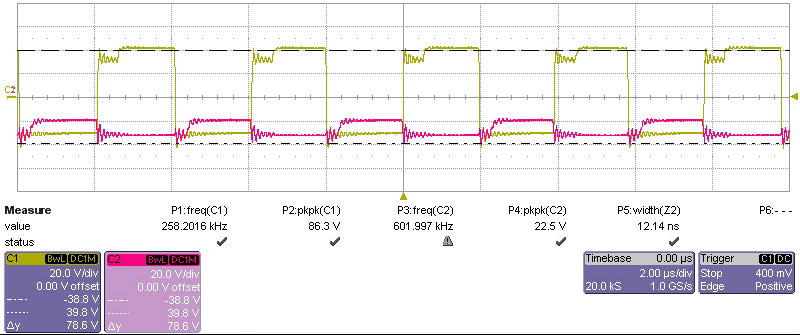
at the inductor input:
initial testing done at +-30V using uf4007 and 1n4148. gate resistor is 10ohm. the amp plays fine without distorting but just wondering if the result i'm getting is optimal?
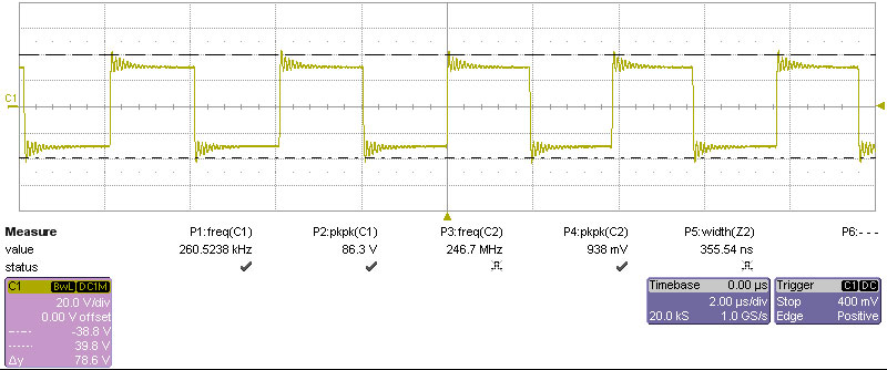
at the mosfet gate:
at the inductor input:
initial testing done at +-30V using uf4007 and 1n4148. gate resistor is 10ohm. the amp plays fine without distorting but just wondering if the result i'm getting is optimal?
guys, anyway suggestion to improve the irs900d performance? i've used the original irs900d with some extra caps bypass but still sticking to the original tl071, cd4049, ir2110 but with irfb5615 and 20uh i got these at the output:
at the mosfet gate:
Look at the gate drive's supply, measure first the largest spurious swing at the gate pin of the FET. Then select cer-cap to comply resosnance frequency.
Then take new curves. And now the largest again, put that MLCC in between driver power supply pin and previously chosen cap. 3 different is enough. you increase efficiency many %!!! and that serial res, lower that to 3R or so...
guys, anyway suggestion to improve the irs900d performance? [...] the amp plays fine without distorting but just wondering if the result i'm getting is optimal?
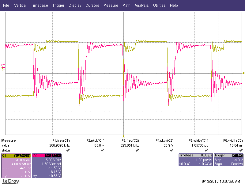
Dead time seems to be very high (400/200 ns), this leads to distortion, however feedback tries to compensate it.
P.S. Nice to see someone who does measurements, and posts it!
Last edited:
first of all guys, i'm not formally educated in electronics so please bear with me. use simple english if you can. still learning here.
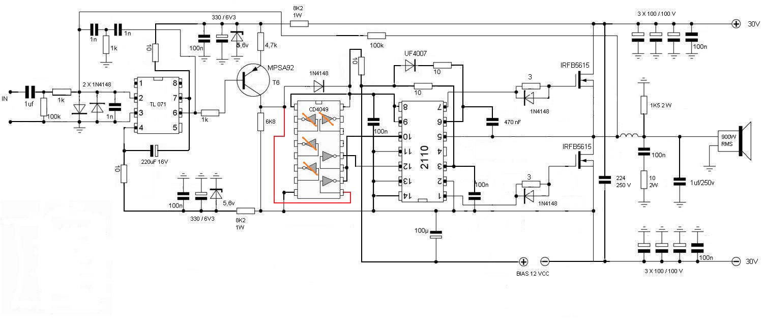
anyway here's the irs900d schematic that i'm using:
the component values are correct and used for this measurement.
measurement points:
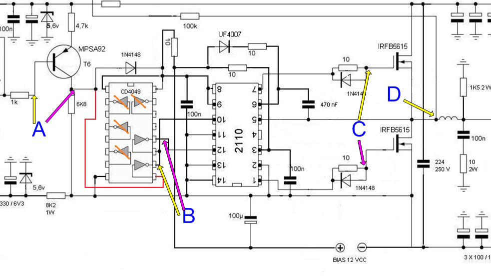
point A:
(removed 100k feedback resistor, ir2110 and mosfet just in case). feed 1khz sine.
point B:
(removed 100k feedback resistor, ir2110 and mosfet just in case). feed 1khz sine.
point C:
no input signal. amp is idle.
point D:
no input signal. amp is idle.
IRF5615: 150V, 35A, 0.039ohm rds(on), gate charge 26nc (typ)/40nc (max), trr 80ns (typ)/120ns (max), qrr 312nc (typ)/468nc (max)
targeted implementation as a subwoofer amp. will be bridging them and feeded with balanced signal from minidsp. target operational voltage is at +-63V. target load is a 4ohm subwoofer with around 1200w or so peak power. the amp would only be seeing <150Hz signal.
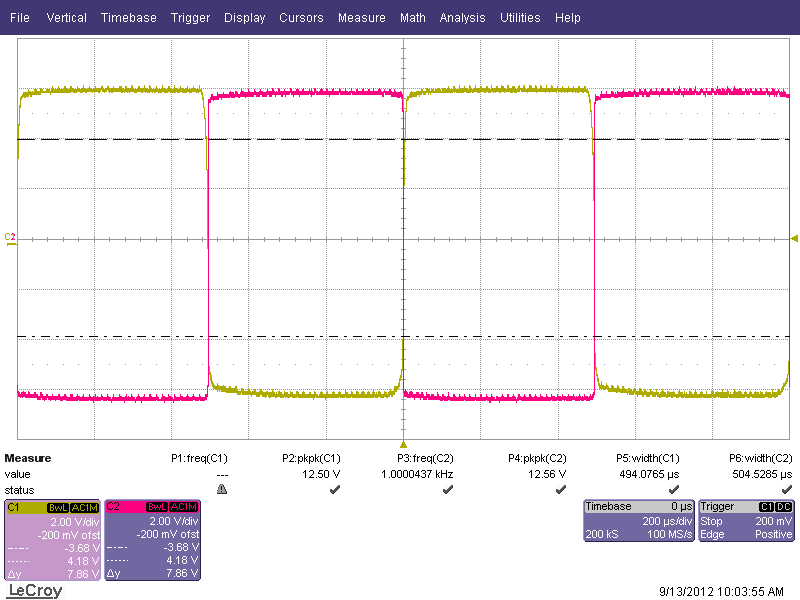
for the most part, i have no idea what i'm supposed to do 😛 (refer above). changed the gate resistor to 3 ohm and the results are posted below.Look at the gate drive's supply, measure first the largest spurious swing at the gate pin of the FET. Then select cer-cap to comply resosnance frequency.
Then take new curves. And now the largest again, put that MLCC in between driver power supply pin and previously chosen cap. 3 different is enough. you increase efficiency many %!!! and that serial res, lower that to 3R or so...
most people don't have access to a scope so it's quite hard to measure anything and for those that do, you guys could be quite intimidating. so it's much easier to just keep quiet and just browse through 😀 any idea on how to optimize the dead time?Dead time seems to be very high (400/200 ns), this leads to distortion, however feedback tries to compensate it.
P.S. Nice to see someone who does measurements, and posts it!
anyway here's the irs900d schematic that i'm using:
the component values are correct and used for this measurement.
measurement points:
point A:
(removed 100k feedback resistor, ir2110 and mosfet just in case). feed 1khz sine.
point B:
(removed 100k feedback resistor, ir2110 and mosfet just in case). feed 1khz sine.
point C:
no input signal. amp is idle.
point D:
no input signal. amp is idle.
IRF5615: 150V, 35A, 0.039ohm rds(on), gate charge 26nc (typ)/40nc (max), trr 80ns (typ)/120ns (max), qrr 312nc (typ)/468nc (max)
targeted implementation as a subwoofer amp. will be bridging them and feeded with balanced signal from minidsp. target operational voltage is at +-63V. target load is a 4ohm subwoofer with around 1200w or so peak power. the amp would only be seeing <150Hz signal.
i don't. though i could try and ask around for it. issit important to have one?Do you have isolated probes?
Hi,paskal9 does by not changing the RSS(8k2) will not affect the whole circuit?cause you're using -/+30,for your initial test. i think 8k2 is for -/+ 90v please correct me if i'm wrong.thank's.
supposedly, yes. but i measured at the TL071 rail and got 4.5V something from using 4.7V zener. so i assumed that the TL071 still get enough voltage for it to work.Hi,paskal9 does by not changing the RSS(8k2) will not affect the whole circuit?cause you're using -/+30,for your initial test. i think 8k2 is for -/+ 90v please correct me if i'm wrong.thank's.
Dead time seems to be very high (400/200 ns),
Hi Pafi
how you say that 400/200 ns . picture shows 12.14ns (1st picture at the mosfet gate)
Hi paskal9,
did you use NE5534 instead of TLO71
Regards
Manoj
Hi Pafi
how you say that 400/200 ns . picture shows 12.14ns (1st picture at the mosfet gate)
Hi paskal9,
did you use NE5534 instead of TLO71
Regards
Manoj
I don't know what is Z2, but I doubt it was the dead time.
The high side gate voltage is added to the output voltage! I indicated actual turn on and off transitions on this picture.

...
Measurements shoud have been made referenced to negative supply, as close to lower mosfet source (or IR2110 GND) as possible. With NOT grounded oscilloscope, of course! Probe grounding lead should be as short as possible.
Last edited:
i don't. though i could try and ask around for it. issit important to have one?
Yes,because you have connected oscilloscope ground to switching bus..Upper mosfet waveforms are not valid without isolated probes
 .
.no i didn't try any NE5534. don't even have any in my parts bin.Hi Pafi
how you say that 400/200 ns . picture shows 12.14ns (1st picture at the mosfet gate)
Hi paskal9,
did you use NE5534 instead of TLO71
Regards
Manoj
tq for the clarification. i was wondering why the high side signal is higher than the low side all this while. Z2 is a previous function that i've since removed.I don't know what is Z2, but I doubt it was the dead time.
The high side gate voltage is added to the output voltage! I indicated actual turn on and off transitions on this picture.
View attachment 301148
...
Measurements shoud have been made referenced to negative supply, as close to lower mosfet source (or IR2110 GND) as possible. With NOT grounded oscilloscope, of course! Probe grounding lead should be as short as possible.
i'll try and scout around for any isolated probes. but slim chances that i'll be able to borrow one.
but from the measurement done i think it's apparent that the dead time could be reduced. any idea on how to optimize the dead time for the design?Yes,because you have connected oscilloscope ground to switching bus..Upper mosfet waveforms are not valid without isolated probes
Show point B with 25 us time div to see deadtime before ir2110.From the measurement done i think it's apparent that the dead time could be reduced. any idea on how to optimize the dead time for the design?
i was afraid someone would say that. i guess that means the dead time are directly affected by the propagation delay time and transition time of the inverter, right?Show point B with 25 us time div to see deadtime before ir2110.
so there's no easy way to change the dead time other than playing around with the VDD and VIN, right?
i was afraid someone would say that. i guess that means the dead time are directly affected by the propagation delay time and transition time of the inverter, right?
so there's no easy way to change the dead time other than playing around with the VDD and VIN, right?
Unfortunately CD4049 is not an ideal comparator, it has a quite low gain (transfer characteristic is not square), this means when it is fed by a slew rate limited signal, then the delay is more, and depends on the slew rate. Measure A also at low time/div! (2 us/div, during normal operation!)
2 more stages of inverter can fasten the transition, and then you have to set a dead time somehow else. CD4049 output current is very asymmetrical, this is a chance to make asymmetric delay = dead time. But first you have to make a correct square!
Hi paskal9,
For any MOSFET switching(conduct) min. volt is 2.5v/3v.below this MOSFET will not conduct. IR2110(logic 5v & VCC 12V supply) high side point it should be 5v with respect to GND and LOW side 5V with respect to -HV supply.The junction point @10V-14V pp signal with respect to GND.For UCD design you need propagation delay @100ns otherwise
the system will not oscillate.
Regards
MANOJ
A way to achieve faster transition is to provide more gain at level shifter. Use lower emitter resistance + z-diode to maintain operation point! A current generator (with j-FET) can be useful to limit max current.
Hi Don2007ksa
Greetings. Is amplifier working with TC4420? Have you tried?
it out
warm regards
andrew lebon
Greetings. Is amplifier working with TC4420? Have you tried?
it out
warm regards
andrew lebon
- Home
- Amplifiers
- Class D
- UCD 25 watts to 1200 watts using 2 mosfets