Will take awhile, I dont have a stabilized psu yet. I want to make one adjustable (9-12-15-18 at least) to try various designs in most comparable conditions.
Let me think, mhmm I see that you're shy a little, don't be affraid to do things more in a radical way ... so:
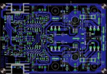
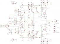
- R33, R34 are half way there as in post #175. You have to move them as in pic, away from the heatsink, now they are just too close, 3 mm would be just fine to avoid short connections, etc.
- C13, C16 polarity-pins should be oriented as C40, C44, I measured the distance from inner pad to close by track and it fits to place perfectly. So put them as in pic #175. Look, if someone is beginner and tries to make an amp as fast as possible, than there are lot of chances to misalign the polarity, cause there is 90° rotation, plus upper and lower elco not having the same orientation. In such cases we always try to make things typically to reduce possibilities of errors.
- C5, C6 are probably silver mica caps, 7,5 mm pins distance. OK, someone would like to use 5 mm pin distance ceramic caps, so please put one extra pad to each cap, that both sizes could fit
- R16, R28, R32, R40 move all four 22 ohm resistors 2 mm in a direction to the center of PCB. Reason? R40, R28 are to close to the fuse metal holder, preventing the shorts at misalignment
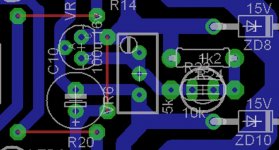
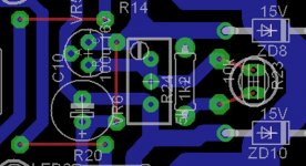
- ZD7-ZD10 should have pad distance of 7,5 mm. Middle two pins of serial zeners holds the current position, outer pins goes closer. Why? You will gain a space to flip R23, R24 horizontally
- R23, R24 should change positions (fliped horizontally). Why? NTC will in that way go closer to the outputs and also will be easily soldered/desoldered when/if PCB is serviced. NTC is glued into the heatsink's hole just bellow its pads. NTC is fixed inside the heatsink and there is better place away from the trimmer for soldering/desoldering
On a first look these are all insignificant changes but certainly makes difference, as assembly is easier and more safe, especially for beginner DIY-ers.
Regards, Andrej 😉
- R33, R34 are half way there as in post #175. You have to move them as in pic, away from the heatsink, now they are just too close, 3 mm would be just fine to avoid short connections, etc.
- C13, C16 polarity-pins should be oriented as C40, C44, I measured the distance from inner pad to close by track and it fits to place perfectly. So put them as in pic #175. Look, if someone is beginner and tries to make an amp as fast as possible, than there are lot of chances to misalign the polarity, cause there is 90° rotation, plus upper and lower elco not having the same orientation. In such cases we always try to make things typically to reduce possibilities of errors.
- C5, C6 are probably silver mica caps, 7,5 mm pins distance. OK, someone would like to use 5 mm pin distance ceramic caps, so please put one extra pad to each cap, that both sizes could fit
- R16, R28, R32, R40 move all four 22 ohm resistors 2 mm in a direction to the center of PCB. Reason? R40, R28 are to close to the fuse metal holder, preventing the shorts at misalignment
- ZD7-ZD10 should have pad distance of 7,5 mm. Middle two pins of serial zeners holds the current position, outer pins goes closer. Why? You will gain a space to flip R23, R24 horizontally
- R23, R24 should change positions (fliped horizontally). Why? NTC will in that way go closer to the outputs and also will be easily soldered/desoldered when/if PCB is serviced. NTC is glued into the heatsink's hole just bellow its pads. NTC is fixed inside the heatsink and there is better place away from the trimmer for soldering/desoldering
On a first look these are all insignificant changes but certainly makes difference, as assembly is easier and more safe, especially for beginner DIY-ers.
Regards, Andrej 😉
as assembly is easier and more safe, especially for beginner DIY-ers.
Thank you for remembering us... 😀

Let me think, mhmm I see that you're shy a little, don't be affraid to do things more in a radical way ... so:
- R23, R24 should change positions (fliped horizontally). Why? NTC will in that way go closer to the outputs and also will be easily soldered/desoldered when/if PCB is serviced. NTC is glued into the heatsink's hole just bellow its pads. NTC is fixed inside the heatsink and there is better place away from the trimmer for soldering/desoldering
On a first look these are all insignificant changes but certainly makes difference, as assembly is easier and more safe, especially for beginner DIY-ers.
Regards, Andrej 😉
Andrey don't you think there is a contradiction in what you wrote : Diy-Beginner and
NTC is glued into the heatsink's hole just bellow its pads. NTC is fixed inside the heatsink and there is better place away from the trimmer for soldering/desoldering
My self, i don't be diy-beginner in soldering and case construction but here i can easily imagine the mounting phase but one time the NTC glued in heathing with previous soldering on pcb....i can't imagine how to desolder this NTC from PCB since it lay in middle of the pcb and here solder pad are quite unreacheable with solder iron?????? Marc who's driving nuts on this spécific point. So for the rest of request i try something....see under.
For ZD 7-10 i try something without modifying the zener part library or create new one....
Attachments
Andrey don't you think there is a contradiction in what you wrote : Diy-Beginner and
Yesss I forgot that there's no pads on top layer 😱 I always have double layer PCB-s, so now we have a problem. NTC would be the best to put in heatsink hole and glue it but how to connect it without using wires mhmmm

Yesss I forgot that there's no pads on top layer 😱 I always have double layer PCB-s, so now we have a problem. NTC would be the best to put in heatsink hole and glue it but how to connect it without using wires mhmmm
What we can built pseudo tracks that bridged bottom and top layer. This can be done by cuted pin from resistors. When this bridge are in place NTC can be soldered in P2P mode. I don't know if my description is clear....
Marc
Here what about i though. In place of NTC there is a hole in PCB (round around NTC) on picture under.
Marc
Yes the same idea here, nice Marc ... but please rotate them 90°, so the NTC is away from the trimmer, especially now when soldering will take place on the top, and put R24 1,2 k by the trimmer. 😎
Look to my previous post regarding 22 pF caps 😉
Ok for 22pf i will modify. Under modification for NTC and previsionnal PSU for TSSA amp (one psu board/TSSA board)
Could you give me a Mouser catalog ref for NTC please?
Could you give me a Mouser catalog ref for NTC please?
Attachments
Last edited:

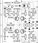
That' mean that i can drive TLP627 by my speaker protection board. this use 12V relay mounted on satellite pcb board? I just have to keep sensing wire comming from amp board output (speaker out)
LC am I right?
Marc
Good morning Idefixes 😉
Just drinking coffee and reading some interesting stuff hehe
Yes, if you have any kind of protection circuit (DC, lowZout, on-delay, fast-off, etc) you can omit output breaker relay (not even buying it 😀) and connect relay drive voltage (usually 12 V potential) to TLP. TLP cuts off output transistors instantly, much faster than any mechanical relay would, simply by interrupting the bias conditions of VAS cascode and consequently the output stage. This solution is well tested and proven in my amps so many times. 😉
Developing an amp is a looong process, especially designing a PCB 😀 so we almost forget to say something about input low pass filter (R1, C1) and input DC offset here (P1, R2, C2). I see that at the input you still have some empty areas, to fill in parts needed 😀
Input DC offset is probably unnecessary cause amp has DC gain set to 1 and those silly little mV's at the input transfered wouldn't do much harm at the output, so we can omit P1, R2, C2 (sch is from SSA).
It would certainly be wise to put R1, C1 on board, values 1 kohm/ 33 pF. Will correct sch later on. 😎
Attachments
Under modification for NTC and previsionnal PSU for TSSA amp (one psu board/TSSA board)
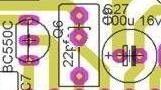
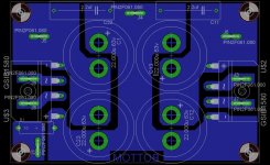
Will you use 88.000 uF for one channel? 😱
Could you give me a Mouser catalog ref for NTC please?
EPCOS - B57164K103J - THERMISTOR, NTC
VISHAY BC COMPONENTS - NTCLE100E3103JB0 - THERMISTOR, NTC
EPCOS - B57703M103G40 - NTC Thermistor
The last one puts everything in a new perspective regarding NTC PCB installation, it can be mounted and soldered the same way as IRFs, no need for two extra pins. 😉
Developing an amp is a looong process, especially designing a PCB 😀 so we almost forget to say something about input low pass filter (R1, C1) and input DC offset here (P1, R2, C2). I see that at the input you still have some empty areas, to fill in parts needed 😀
Input DC offset is probably unnecessary cause amp has DC gain set to 1 and those silly little mV's at the input transfered wouldn't do much harm at the output, so we can omit P1, R2, C2 (sch is from SSA).
It would certainly be wise to put R1, C1 on board, values 1 kohm/ 33 pF. Will correct sch later on. 😎
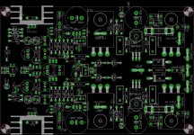
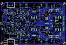
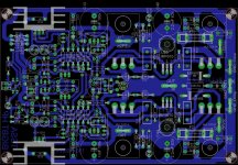
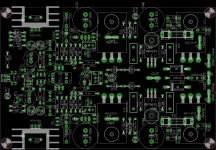
Here we go, R1/C1 value are these from SSA schematic form moment until value is fixed. The add of latest component don't let keep the nice input area symetry we had in previous version.
Marc
Attachments
- Home
- Amplifiers
- Solid State
- TSSA - The Simplest Symmetrical Amplifier