Hi, waiting to test the sound of the amp in reality, I post here some curves of the item in different configurations (as shown on each curve):
Attachments
-
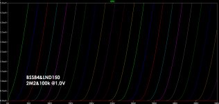 Curves-BSS84&LND150-2M2&100k-@1,0V.jpg190.9 KB · Views: 304
 -
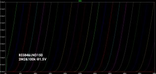 Curves-BSS84&LND150-2M2&100k-@1.5V.jpg193.6 KB · Views: 301
 -
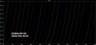 Curves-BSS84&LND150-2M2&100k-@2,0V.jpg194.8 KB · Views: 289
 -
 Curves-BSS84&LND150-2M2&100k-@2,5V.jpg189.8 KB · Views: 281
 -
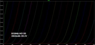 Curves-BSS84&LND150-2M2&68k-@2,5V.jpg165.9 KB · Views: 285
 -
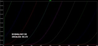 Curves-BSS84&LND150-2M2&33k-@2,5V.jpg121.9 KB · Views: 156
 -
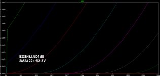 Curves-BSS84&LND150-2M2&22k-@2,5V.jpg111.1 KB · Views: 158
 -
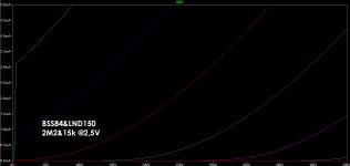 Curves-BSS84&LND150-2M2&15k-@2,5V.jpg103.6 KB · Views: 163
late to game ...... Boyz in tube Forum beat that Issue to death, our brave George was certainly one of them
Trioderizer arrangement is well known, while fact that you're driving it with/to Source (with "upside-down" mosfet) is Cherry on top
in fact, Papa's DEF circuit, (as origin in thinking of ) in my SET amp - where depletion mode part is replaced with Schaded mosfet, is sorta same arrangement - drive is pretty much hybrid of gate/source drive, at least when thinking of Schaded mosfet modulation
in any case, nice thinking
just use - in simulation, load value of much lower size, that's more like it is in real life
if preamp stage is in case, think of no more than 50-100K, as usual Rin of next stage (amp)
Thank you for your intervention Zen Mod,
indeed, in post #1 I cited George and in post #13 I cited SpreadSpectrum as inspiration for the two different circuits shown on each post.
May I ask you to suggest me a pair of n and p mosfets to use this circuit as single gain stage, single ended power amp? Something being able to give around 35W on 8 Ohm would be perfect, as I have a pair of 48V 10A power supplies.
Thank you in advance
Last edited:
usual suspects in Papaland are IRFP240/9240 , slightly more complementary being 240/9140 (as always written by ilimzn)
to keep them happy - do not exceed 35W of dissipation, up to 50W if you're really sure in thermal arrangement - meaning exquisite heatsinking
slightly sturdier is IRFP150 (practically being two IRFP240 in one case) , but problem is - there is no close P channel cousin of it, at least not to my knowledge
Thank you very much Zen Mod!
Good thing about the pair is that they do not need to be paired, as the bottom pmosfet only sees a fraction (determined by the ratio of the feedback) of the voltage, so a fraction of the power. The pmosfet only needs to have a low Ciss and an high current handling, whilst nmosfet need to take care of most part of the voltage swing plus current.
I will check what you suggested. May I ask you what parameters I need to search on mouser to find other similar mosfets? Thanks!
This one: https://www.diyaudio.com/forums/att...-curves-channel-dmos-triodized-gain-stage-jpg
Top nmosfet need to swing 50V and 10A, bottom pmosfet can swing just 10V and 10A with a small Ciss. Then of course a reliable CCS, but should be easy to be found.
Thank you!
Top nmosfet need to swing 50V and 10A, bottom pmosfet can swing just 10V and 10A with a small Ciss. Then of course a reliable CCS, but should be easy to be found.
Thank you!
for N channel, I''m lazy so IRFP150 is always first on my mind
for P channel - dunno what small Ciss mean to you 🙂
though, it really depends what intended previous stage is ( matter of Rout) - you can always put small buffer in front of P channel gate, so matter of Ciss isn't so critical anymore
if thinking big, time is to resort to IXYS pucks
for P channel - dunno what small Ciss mean to you 🙂
though, it really depends what intended previous stage is ( matter of Rout) - you can always put small buffer in front of P channel gate, so matter of Ciss isn't so critical anymore
if thinking big, time is to resort to IXYS pucks
Thank you again Zen Mod!
Very nice device! https://www.vishay.com/docs/91203/91203.pdf
The total resistance of the voltage divider must be lower to drive the gate of the device, I would say no more than 500 Ohm total.
Voltage ratio can be way lower as well, because there's just need of a gain of... 48 Vpp / 2 Vrms = 48/5,64 = 8,5. Let's say 10.
I've selected on mouser for:
- p-mosfet TO220
- Id continuous at least 10 A;
This one is the one with the lowest Ciss:
https://www.mouser.it/datasheet/2/196/Infineon_IRF9Z24N_DataSheet_v01_01_EN-1732681.pdf
Being directly connected to a DAC (through a volume pot), 350 pF are low enough to guarantee a good performance.
Do you think it would be easier to implement the second circuit ( https://www.diyaudio.com/forums/att...triode-curves-channel-dmos-zintolo-se-amp-jpg ), so that the gain stage can manage some orders of magnitude less of current (so also be easier to drive), and then DC coupled to one or more DC coupled and CCS loaded source followers to manage the current?
In that case I'd drive the n-mosfet and the p-mosfet would give feedback.
In that case I'd drive the n-mosfet and the p-mosfet would give feedback.
Thanks Zen Mod,
I will then follow your suggestion and try to develop the second option.
Driver could be a LSK389 as matched nmosfet with another small pmosfet on bottom and a resistor as load, then a big source follower to drive the speaker.
I will then follow your suggestion and try to develop the second option.
Driver could be a LSK389 as matched nmosfet with another small pmosfet on bottom and a resistor as load, then a big source follower to drive the speaker.
Here are a couple of other options for triode-like behavior using mosfets and jfets..
Simulated Triode (Schade) SE OL Headphone Amp
Simulated Triode (Schade) SE OL Headphone Amp
Looks like a fun idea. I don't have any helpful comments other than I'm interested in how this goes.
I played a bit with LTSpice while waiting to have again a space to mount and test circuits.
With a ZVP3310 as pmosfet source follower, J201 as nfet gain stage and LND150 as CCS set at 1.6 mA, 100k&22k feedback to J201's gate, 2Vrms input and 0-35V power sypply it swings between 3 and 34V (10.8 Vrms) with the following harmonic content.
I would like to couple a SS power amp to it, can anyone suggest me something simple to simulate and then build the amp?
Thanks in advance
Roberto
With a ZVP3310 as pmosfet source follower, J201 as nfet gain stage and LND150 as CCS set at 1.6 mA, 100k&22k feedback to J201's gate, 2Vrms input and 0-35V power sypply it swings between 3 and 34V (10.8 Vrms) with the following harmonic content.
Code:
Harmonic    Frequency     Fourier     Normalized     Phase      Normalized
 Number       [Hz]       Component     Component    [degree]    Phase [deg]
    1       1.000e+03    1.526e+01    1.000e+00       -0.02°        0.00°
    2       2.000e+03    7.431e-03    4.871e-04      -85.24°      -85.22°
    3       3.000e+03    3.240e-04    2.124e-05       44.89°       44.91°
    4       4.000e+03    1.047e-04    6.864e-06      175.57°      175.59°
    5       5.000e+03    5.063e-05    3.319e-06      -90.70°      -90.67°
    6       6.000e+03    2.539e-05    1.664e-06       -0.48°       -0.45°
    7       7.000e+03    1.299e-05    8.514e-07       89.19°       89.21°
    8       8.000e+03    6.717e-06    4.403e-07      179.53°      179.56°
    9       9.000e+03    3.565e-06    2.337e-07      -90.47°      -90.45°
Total Harmonic Distortion: 0.048759%(0.048752%)
I would like to couple a SS power amp to it, can anyone suggest me something simple to simulate and then build the amp?
Thanks in advance
Roberto
Attachments
Thank you @thorstenlarsen !
What is the benefit of a nmosfet with CCS to the negative rail vs pmosfet with CCS to the positive rail?
The reason of my question is that I have the CCS to the positive rail on the preamp (so good rejection to PSU noise) and I would keep the same to the "power follower" to improve the noise rejection. Of course I would ground the negative rais (as in the schematic) and refer the speaker to ground as well.
That would be fine! The main point is to have the speaker in parallel to the active transistor, not in parallel to the current source. N-channel FET’s are cheaper and more available though, and might be
better.
Thorsten
better.
Thorsten
amp itself is not feeling difference of where load return is , as long it is functional GND
be it "real" one or virtual
any enough unmovable potential can be used as "GND"
so, speaker return can go to real GND or to other rail , as long rail is stiff enough
resulting noise and ripple at speaker terminals is separate issue
be it "real" one or virtual
any enough unmovable potential can be used as "GND"
so, speaker return can go to real GND or to other rail , as long rail is stiff enough
resulting noise and ripple at speaker terminals is separate issue
- Home
- Amplifiers
- Solid State
- Triode-like curves from a n-channel DMOS (and not only)