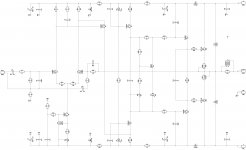
Just for fun - my version. The front-end from VHex amplifier, slightly adapted for line stage requirements.
Basic parameters:
OLG @ 1KHz = 95db
THD @ 1KHz open loop = 0.04%
CLG @ 1KHz = 12db
THD @ 1KHz = 0.00006%
Output impedance = 1 ohm
ULGF = 7.5MHz
No Miller compensation (allowed by current-driven VAS).
Fast and clean step response.
In fact - same grade as the one from Apex above. Key difference - I like this compensation scheme sound-wise. Ultimate clarity.
Cheers,
Valery
I've built this version and am very happy with it.
As a preamp?I've built this version and am very happy with it.
Member
Joined 2009
Paid Member
symmetric LTP input and ... Could be basis of a good MOSFET amp probably by placing hexFETs at outputs ...
http://www.diyaudio.com/forums/solid-state/239418-tgm7-amplifier-based-greg-ball-ska.html
Attachments
Well, let's take another look at the story, shall we?knowledgeable experienced people are posting their comments, based on either some "well known" general information, or some very rough assumptions.
The huge weakness of this design is that almost all the voltage gain comes from the output stage; that voltage gain is obtained by having each output transistor work into a very high impedance (the collector impedance of it's complimentary partner).
Now, if you load the output, that huge load impedance is gone. When it falls, so does the open-loop gain. The lower the load impedance, the worse the problem is.
If, for example, you connect 32 ohm headphones to the output, the voltage gain of each output transistor is about one-third; 0.33, or -10 dB! The gain is less than unity, it's actually throwing away gain, like a potentiometer!
This is because each output device has an 82 ohm emitter; its voltage gain is therefore a bit lower than (32 ohms/82 ohms). Lower because there is also the dynamic resistance of the emitter-base junction to deal with, which adds to the 82 ohm resistance.
There isn't a whole lot of voltage gain happening in the input stage, either. This is because there is rather a small voltage drop occurring across those 3.3k collector load resistors. The voltage gain of a transistor stage is directly proportional to the DC voltage across the collector resistor - keep this voltage low, and the voltage gain will be low, too.
Okay, that's what's happening in my words, but how do you know if I'm talking through my hat? Maybe I'm yet another nitwit spouting total nonsense on the Internet?
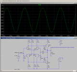
So I wasted 15 minutes of my life entering this schematic into LTSpice. The exact transistors in this amp aren't included in LTSpice, and I didn't want to waste even more of my time simulating a design of dubious quality, so I used small-signal silicon epitaxial transistors from the same family.
If anyone is feeling particularly picky, I'm attaching the .asc (simulation) file. Cordell Audio (dot com) has LTSpice models for the BC550C and BC560C. Please feel free to plug in the Cordell Audio models, and re-run the simulation.
There is one other change to the schematic; I used a 100uF cap to remove all the (AC) negative feedback, so what you see is the full open-loop gain of the circuit.
Note also that the sine wave input signal is 1 mV peak. Look at the graphs, read off the peak value of the output in millivolts, and that is the open-loop gain. If you see, let's say, 6 volt peaks on the output, the voltage gain would be (6000 mV/ 1 mV), or 6000 times.
So what did LTSpice say? When the output is unloaded (best case) the voltage gain is 1200 times; Nearly 62 dB. Not great, considering the complexity of the circuit, but at least not utterly horrible, either. (I unloaded the circuit by making the load resistance very, very large - look at the value in the schematic.)
(NOTE: The screenshot says 2400 times instead of 1200 times; I forgot that when you tell LTSpice "1 mV", it actually spits out 2mV peak-to-peak. Actual gain is half of what I wrote on the screenshots, which is 1200 in this case.)
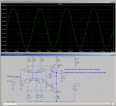
The second screenshot shows what happens if you connect 32 ohm headphones to the output. This is a typical impedance for generic portable-device headphones, and probably a worst-case load for this little preamp. The input is still 2 mV peak-to-peak, the output voltage (open loop) is only 30 mV(!) The open-loop voltage gain is only about 15 times, around 24 dB!
An open-loop gain of 15 times? This might have been passable if it was obtained from one single primitive triode valve in 1915. But from six modern high-performance silicon small-signal transistors in 2016? That's so bad, it's absurd.
I know nothing about the designer of this circuit, and I don't want to; this is not a personal vendetta. But failing to buffer the voltage gain stage makes no design sense at all, unless this circuit was intended to never have any load on the output. (Well, that makes no sense at all, either.)
Anyone can have a bad day, and perhaps the designer just had a really, really bad day when he/she put together this particular circuit. Perhaps all his/her other circuits are brilliant. I don't know.
But whatever the cause, this is a poorly designed circuit. Buffering the output stage would make it a lot better.
-Gnobuddy
Attachments
Thank you for the in-depth evaluation Gnobuddy.
Perhaps Valery can buffer the output stage or make the necessary changes.
Perhaps Valery can buffer the output stage or make the necessary changes.
Gnobuddy,
I used that circuit as a pre-amp for a 100kohm input impedance of the Pass M2. For that purpose, it worked quite well. It was never designed to be a headphone amp. I got sound out of it just to check - but did not check to see how good it sounded with a low impedance load.
The designer is ApexAudio (a.k.a. Mile Slakovic) - who, judging by his prolific output of great sounding amps (about one or two designs a month) with a huge following of builders in this thread, I think he would know a thing or two about audio amp design. I built it and tested it - the gain is around 10dB with 100kohm load. Who cares if the gain is 1200x without a load? Listening to it, it sounds quite distortion free and does what is asked of it. Sorry you felt the need to waste 15 minutes of your life entering it into Spice without the correct models.
If you want to see a partial list of Apex Audio amps look here:
http://www.diyaudio.com/forums/solid-state/292226-directory-apex-audio-amplifiers.html
I used that circuit as a pre-amp for a 100kohm input impedance of the Pass M2. For that purpose, it worked quite well. It was never designed to be a headphone amp. I got sound out of it just to check - but did not check to see how good it sounded with a low impedance load.
I know nothing about the designer of this circuit, and I don't want to; this is not a personal vendetta. But failing to buffer the voltage gain stage makes no design sense at all, unless this circuit was intended to never have any load on the output. (Well, that makes no sense at all, either.) Anyone can have a bad day, and perhaps the designer just had a really, really bad day when he/she put together this particular circuit. Perhaps all his/her other circuits are brilliant. I don't know.
The designer is ApexAudio (a.k.a. Mile Slakovic) - who, judging by his prolific output of great sounding amps (about one or two designs a month) with a huge following of builders in this thread, I think he would know a thing or two about audio amp design. I built it and tested it - the gain is around 10dB with 100kohm load. Who cares if the gain is 1200x without a load? Listening to it, it sounds quite distortion free and does what is asked of it. Sorry you felt the need to waste 15 minutes of your life entering it into Spice without the correct models.
If you want to see a partial list of Apex Audio amps look here:
http://www.diyaudio.com/forums/solid-state/292226-directory-apex-audio-amplifiers.html
Well, let's take another look at the story, shall we?
The huge weakness of this design is that almost all the voltage gain comes from the output stage; that voltage gain is obtained by having each output transistor work into a very high impedance (the collector impedance of it's complimentary partner).
Now, if you load the output, that huge load impedance is gone. When it falls, so does the open-loop gain. The lower the load impedance, the worse the problem is.
If, for example, you connect 32 ohm headphones to the output, the voltage gain of each output transistor is about one-third; 0.33, or -10 dB! The gain is less than unity, it's actually throwing away gain, like a potentiometer!
This is because each output device has an 82 ohm emitter; its voltage gain is therefore a bit lower than (32 ohms/82 ohms). Lower because there is also the dynamic resistance of the emitter-base junction to deal with, which adds to the 82 ohm resistance.
There isn't a whole lot of voltage gain happening in the input stage, either. This is because there is rather a small voltage drop occurring across those 3.3k collector load resistors. The voltage gain of a transistor stage is directly proportional to the DC voltage across the collector resistor - keep this voltage low, and the voltage gain will be low, too.
Okay, that's what's happening in my words, but how do you know if I'm talking through my hat? Maybe I'm yet another nitwit spouting total nonsense on the Internet?
So I wasted 15 minutes of my life entering this schematic into LTSpice. The exact transistors in this amp aren't included in LTSpice, and I didn't want to waste even more of my time simulating a design of dubious quality, so I used small-signal silicon epitaxial transistors from the same family.
If anyone is feeling particularly picky, I'm attaching the .asc (simulation) file. Cordell Audio (dot com) has LTSpice models for the BC550C and BC560C. Please feel free to plug in the Cordell Audio models, and re-run the simulation.
There is one other change to the schematic; I used a 100uF cap to remove all the (AC) negative feedback, so what you see is the full open-loop gain of the circuit.
Note also that the sine wave input signal is 1 mV peak. Look at the graphs, read off the peak value of the output in millivolts, and that is the open-loop gain. If you see, let's say, 6 volt peaks on the output, the voltage gain would be (6000 mV/ 1 mV), or 6000 times.
So what did LTSpice say? When the output is unloaded (best case) the voltage gain is 1200 times; Nearly 62 dB. Not great, considering the complexity of the circuit, but at least not utterly horrible, either. (I unloaded the circuit by making the load resistance very, very large - look at the value in the schematic.)
(NOTE: The screenshot says 2400 times instead of 1200 times; I forgot that when you tell LTSpice "1 mV", it actually spits out 2mV peak-to-peak. Actual gain is half of what I wrote on the screenshots, which is 1200 in this case.)
The second screenshot shows what happens if you connect 32 ohm headphones to the output. This is a typical impedance for generic portable-device headphones, and probably a worst-case load for this little preamp. The input is still 2 mV peak-to-peak, the output voltage (open loop) is only 30 mV(!) The open-loop voltage gain is only about 15 times, around 24 dB!
An open-loop gain of 15 times? This might have been passable if it was obtained from one single primitive triode valve in 1915. But from six modern high-performance silicon small-signal transistors in 2016? That's so bad, it's absurd.
I know nothing about the designer of this circuit, and I don't want to; this is not a personal vendetta. But failing to buffer the voltage gain stage makes no design sense at all, unless this circuit was intended to never have any load on the output. (Well, that makes no sense at all, either.)
Anyone can have a bad day, and perhaps the designer just had a really, really bad day when he/she put together this particular circuit. Perhaps all his/her other circuits are brilliant. I don't know.
But whatever the cause, this is a poorly designed circuit. Buffering the output stage would make it a lot better.
-Gnobuddy
Hi Gnobuddy,
I am not experienced, so need a suggestion here. Will the APEX pre-amp design work well for power amplifiers with i/p impedance of 10k to 100k? As just a pre-amp with volume control (never as headphone amp) as an amplifying stage between low voltage sources like some mobiles (0.6V o/p) and power amplifier (with 24k i/p impedance) which need 2.5V to reach full power.
-Hindalco
In reality everything is different than it really is.
Totally agree!
Please don't connect anything with 32 ohm input impedance to this circuit!
This is NOT a headphone amp.
This is the line stage, expected to work in front of the power amplifier.
Where did you see the power amplifier with 32 ohm input impedance?
However, you're missing 1K resistor in resistor to ground in your feedback network, so your setup is unity gain - that's where your -10db is coming from. With the right divider values, it's still 10db positive.
As I mentioned earlier, with 10 Kohm ... 100 Kohm load it works no problem.
Both yourself and JMFahey may be surprised, but I stress this point once again - because of the deep negative feedback, the output impedance of this line stage is less than 10 ohm. Which is perfectly fine to drive the power amp's input.
How come it's that low, providing the VAS is a common-emitter push-pull?
The reason is well described by Cherry and Cambrell in their article "Output Resistance and Intermodulation Distortion of Feedback Amplifiers" (April 1982) - available in AES library.
I will take a liberty to quote a couple of paragraphs (damn, I have to re-type them 🙂):
"... CC (emitter follower) output stages are known to be better than CE stages when a low output resistance is desirable or when the load is known to be capacitive.
Unfortunately it ain't so.
...
With the same constraints of equal load capacitance, stability margin, and quiescent point, a CE stage with feedback gives the same output resistance as a CC stage with feedback.
The source of misconception is in the often quoted result that the output resistance of an amplifier with feedback is the open-loop output resistance of the output stage divided by loop gain plus unity. This is again ain't so. The correct expression ... involves not the ordinary loop gain such as used in a Nyquist diagram to determine system stability, but the value the loop gain would have had if the load had been open circuited. For low-output-resistance stages the two values of loop gain are nearly equal, but for high-output-resistance stages the open-circuit-load loop gain is much larger than the ordinary loop gain and offsets the larger open-loop output resistance."
I recommend to read the full article to every practicing designer - free for AES members now.
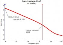
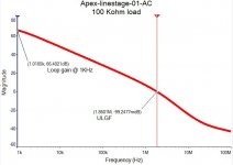
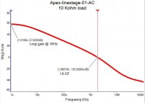
Attached images illustrate the feedback loop gain with the LOOP CLOSED:
1) no external load (LG = 67.6db, CLG = 12db -> OLG = 79.6db)
2) 100 Kohm external load (LG = 66.4db, CLG = 12db -> OLG = 78.4db)
3) 10 Kohm external load (LG = 57.8db, CLG = 12db -> OLG = 69.8db)
No problem, right?
Of course, if we need a headphone amplifier, we need a power buffer at the output - I have mentioned my design configuration, suitable for the purpose.
Cheers,
Valery
If, for example, you connect 32 ohm headphones to the output, the voltage gain of each output transistor is about one-third; 0.33, or -10 dB! The gain is less than unity, it's actually throwing away gain, like a potentiometer!
Totally agree!
Please don't connect anything with 32 ohm input impedance to this circuit!
This is NOT a headphone amp.
This is the line stage, expected to work in front of the power amplifier.
Where did you see the power amplifier with 32 ohm input impedance?
However, you're missing 1K resistor in resistor to ground in your feedback network, so your setup is unity gain - that's where your -10db is coming from. With the right divider values, it's still 10db positive.
As I mentioned earlier, with 10 Kohm ... 100 Kohm load it works no problem.
Both yourself and JMFahey may be surprised, but I stress this point once again - because of the deep negative feedback, the output impedance of this line stage is less than 10 ohm. Which is perfectly fine to drive the power amp's input.
How come it's that low, providing the VAS is a common-emitter push-pull?
The reason is well described by Cherry and Cambrell in their article "Output Resistance and Intermodulation Distortion of Feedback Amplifiers" (April 1982) - available in AES library.
I will take a liberty to quote a couple of paragraphs (damn, I have to re-type them 🙂):
"... CC (emitter follower) output stages are known to be better than CE stages when a low output resistance is desirable or when the load is known to be capacitive.
Unfortunately it ain't so.
...
With the same constraints of equal load capacitance, stability margin, and quiescent point, a CE stage with feedback gives the same output resistance as a CC stage with feedback.
The source of misconception is in the often quoted result that the output resistance of an amplifier with feedback is the open-loop output resistance of the output stage divided by loop gain plus unity. This is again ain't so. The correct expression ... involves not the ordinary loop gain such as used in a Nyquist diagram to determine system stability, but the value the loop gain would have had if the load had been open circuited. For low-output-resistance stages the two values of loop gain are nearly equal, but for high-output-resistance stages the open-circuit-load loop gain is much larger than the ordinary loop gain and offsets the larger open-loop output resistance."
I recommend to read the full article to every practicing designer - free for AES members now.
Attached images illustrate the feedback loop gain with the LOOP CLOSED:
1) no external load (LG = 67.6db, CLG = 12db -> OLG = 79.6db)
2) 100 Kohm external load (LG = 66.4db, CLG = 12db -> OLG = 78.4db)
3) 10 Kohm external load (LG = 57.8db, CLG = 12db -> OLG = 69.8db)
No problem, right?
Of course, if we need a headphone amplifier, we need a power buffer at the output - I have mentioned my design configuration, suitable for the purpose.
Cheers,
Valery
Attachments

Thank you for the in-depth evaluation Gnobuddy.
Perhaps Valery can buffer the output stage or make the necessary changes.
Mine is buffered 😉
Hi Gnobuddy,
I am not experienced, so need a suggestion here. Will the APEX pre-amp design work well for power amplifiers with i/p impedance of 10k to 100k? As just a pre-amp with volume control (never as headphone amp) as an amplifying stage between low voltage sources like some mobiles (0.6V o/p) and power amplifier (with 24k i/p impedance) which need 2.5V to reach full power.
-Hindalco
Yes, that's exactly what this preamp from Apex is aimed for.
Yes, that's exactly what this preamp from Apex is aimed for.
Thank you so much for kindly answer vzaichenko.
Hindalco
This circuit would benefit from adding four 100ohm emitter degeneration resistors to reduce the input transconductance. Then, the compensation caps might be reduced to improve the slew rate. The fet version can be left as it is, because the jfets have less intrinsic transconductance than bipolars have.
This circuit would benefit from adding four 100ohm emitter degeneration resistors to reduce the input transconductance. Then, the compensation caps might be reduced to improve the slew rate. The fet version can be left as it is, because the jfets have less intrinsic transconductance than bipolars have.
Exactly - that was my thought as well in the very beginning, although I didn't mention it. Degeneration would make the whole thing less "nervous", allowing lighter compensation and hopefully making it somewhat even nicer sound-wise.
That's what I did in my circuit.
The designer is ApexAudio (a.k.a. Mile Slakovic) - who, judging by his prolific output of great sounding amps (about one or two designs a month) with a huge following of builders in this thread, I think he would know a thing or two about audio amp design. I built it and tested it - the gain is around 10dB with 100kohm load. Who cares if the gain is 1200x without a load? Listening to it, it sounds quite distortion free and does what is asked of it.
 Apex amps sound wonderful and that thread is a candy store for diyers. I am sure this preamp too must be sounding great if used in linestage.
 X does it add any improvement/ coloration to sound, since you have listened to both versions (with and without pre-amp...)
reg
Prasi
Last edited:
VHex Headphone Edition schematic
OK, here is the schematic, based on VHex 1.1, amended for running as an all-around precision headphone amp.
Rails are +/-24V DC.
Set DC offset to zero, set the bias to 100mA, check/correct the offset once again, set the bias to 200mA. Make sure the heatsinks are good enough for running with constant 10W dissipation per channel. Use some DC offset protection at the output.
Have fun 😉
Valery, can you post or provide a link to a the VHex 1.1 schematic so we can see what needs to be changed on abetir's board in order to use the circuit you posted in post number 126?
Thanks.
OK, here is the schematic, based on VHex 1.1, amended for running as an all-around precision headphone amp.
Rails are +/-24V DC.
Set DC offset to zero, set the bias to 100mA, check/correct the offset once again, set the bias to 200mA. Make sure the heatsinks are good enough for running with constant 10W dissipation per channel. Use some DC offset protection at the output.
Have fun 😉
Attachments
This circuit would benefit from adding four 100ohm emitter degeneration resistors to reduce the input transconductance. Then, the compensation caps might be reduced to improve the slew rate. The fet version can be left as it is, because the jfets have less intrinsic transconductance than bipolars have.
Hi John,
Will this result in any audible improvement?
reg
Prasi
X does it add any improvement/ coloration to sound, since you have listened to both versions (with and without pre-amp...)
reg
Prasi
Prasi,
It is totally transparent - I cannot tell it does anything to the sound other than boost the output from the M2's 14dB of gain. Measurement of the frequency response at the speaker via mic shows that it is transparent as well.
OK, here is the schematic, based on VHex 1.1, amended for running as an all-around precision headphone amp.
Rails are +/-24V DC.
Set DC offset to zero, set the bias to 100mA, check/correct the offset once again, set the bias to 200mA. Make sure the heatsinks are good enough for running with constant 10W dissipation per channel. Use some DC offset protection at the output.
Have fun 😉
What happened to the circuit in post 126 that uses C3503 and A1381 for the outputs? Is it not any good?
That's the circuit I'm interested in trying to alter Albert's layout for if possible.
By the way, I sent Albert a PM yesterday for the layout file and haven't heard back from him.
- Home
- Source & Line
- Analog Line Level
- Transistor Preamp