hfe is current gain. At some point in the circuit that has to be translated into voltage gain, usually by dumping all that current into a large impedance.These transistors have Hfe in the 470 range. Isn't open loop gain on two stages 220k?
I haven't simulated the circuit in LTSpice, or done formal calculations, so perhaps I'm wrong. But it looks as though the relatively low collector loads (3.3k) will shunt away (waste) a fair bit of the current gain.
The complimentary output devices effectively have current-source loads, which is good for high voltage gain; but now you have a very high output impedance there, and there's nothing to buffer the output! So if you connect any reasonable load to the output, the open-loop gain of the circuit drops like a rock.
There were some truly brilliant analogue designers behind many of the wonderful "classic" op-amps we are so casual about today. IMO, the performance of even an old-school NE5532 or TLO72 is pretty hard to match with a discrete circuit.
-Gnobuddy
There were some truly brilliant analogue designers behind many of the wonderful "classic" op-amps we are so casual about today. IMO, the performance of even an old-school NE5532 or TLO72 is pretty hard to match with a discrete circuit.
-Gnobuddy
Of course, and that´s the point.
But armchair designers try to beat them throwing a handful of parts over the table and claiming superiority 🙄
These transistors have Hfe in the 470 range. Isn't open loop gain on two stages 220k?
That´s *current* gain, not voltage gain which is implied in the "open loop" expression.
I calculate (in my mind, I do not simulate) available gain about 30/40X on the differential stage and 40X in the scond one, so we are in the order of some 1200/1400X open loop gain, 30 something dB, a FAR cry from 220k , which would have been reasonable in an old Op Amp, think 741 .
Guys, in many cases, knowledgeable experienced people are posting their comments, based on either some "well known" general information, or some very rough assumptions.
You are just confusing the less experienced members, reading your comments and making decisions, based on the very rough, inaccurate information you provide.
Now, let's see what the truth is.
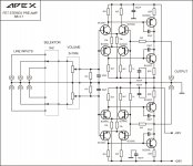
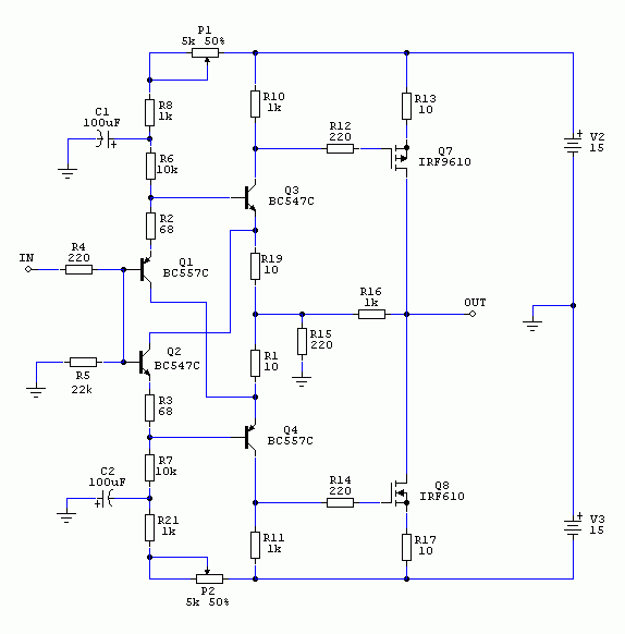
I'm talking about schematic from the post #7 (top picture - bjt input version, attached here as well for your reference).
OLG @ 1KHz = 80db (far from 30db, mentioned above)
THD @ 1KHz open loop = 0.03% (not bad at all for open loop with such gain)
ULGF = 1.8MHz
CLG @ 1KHz = 12db (as set by the FB network)
THD @ 1KHz = 0.00011% (not enough for somebody?)
Output impedance = 9.7 ohm (more than "low enough" for driving some 10...100 Kohm input impedance of the power amp). Don't forget - NFB reduces the output impedance.
Conclusion - perfect for the purpose.
Please ... let's try to keep more attention to detail.
Cheers,
Valery
You are just confusing the less experienced members, reading your comments and making decisions, based on the very rough, inaccurate information you provide.
Now, let's see what the truth is.
I'm talking about schematic from the post #7 (top picture - bjt input version, attached here as well for your reference).
OLG @ 1KHz = 80db (far from 30db, mentioned above)
THD @ 1KHz open loop = 0.03% (not bad at all for open loop with such gain)
ULGF = 1.8MHz
CLG @ 1KHz = 12db (as set by the FB network)
THD @ 1KHz = 0.00011% (not enough for somebody?)
Output impedance = 9.7 ohm (more than "low enough" for driving some 10...100 Kohm input impedance of the power amp). Don't forget - NFB reduces the output impedance.
Conclusion - perfect for the purpose.
Please ... let's try to keep more attention to detail.
Cheers,
Valery
Attachments
Thanks for doing that Valery. Explains why it sounds pretty darn good. I even connected my headphones to it and seems to drive them just fine so confirms the output impedance is low.
AWire - VHex-based line stage
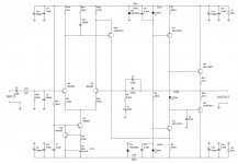
Just for fun - my version. The front-end from VHex amplifier, slightly adapted for line stage requirements.
Basic parameters:
OLG @ 1KHz = 95db
THD @ 1KHz open loop = 0.04%
CLG @ 1KHz = 12db
THD @ 1KHz = 0.00006%
Output impedance = 1 ohm
ULGF = 7.5MHz
No Miller compensation (allowed by current-driven VAS).
Fast and clean step response.
In fact - same grade as the one from Apex above. Key difference - I like this compensation scheme sound-wise. Ultimate clarity.
Cheers,
Valery
Attachments
Last edited:
Huh ... just thought - this one can be built right on VHex+ boards - just don't install the output devices, remove the spreader and put some jumper wires 😉
No.These transistors have Hfe in the 470 range. Isn't open loop gain on two stages 220k?
Open loop gain is a matter of voltage gain, not current gain.
Huh ... just thought - this one can be built right on VHex+ boards - just don't install the output devices, remove the spreader and put some jumper wires 😉
I was thinking the same thing. It would be a pretty decent headphone amp too. What's max power output from KSA/KSC's I wonder?
Only drawback is the board is rather large for a little preamp. It would be great if a PCB layout master could put out a design for this with through holes in a small footprint. Those are amazingly low distortion figures.
Last edited:
No.
Open loop gain is a matter of voltage gain, not current gain.
Understood - this was already pointed out several posts above.
I was thinking the same thing. It would be a pretty decent headphone amp too. What's max power output from KSA/KSC's I wonder?
Only drawback is the board is rather large for a little preamp. It would be great if a PCB layout master could put out a design for this with through holes in a small footprint. Those are amazingly low distortion figures.
There is a compact TH layout in Abetir's thread, where VHex appeared for the first time. It's closer to square shape and rather small.
In this configuration it can drive some 100mW into 300 ohm headphones.
But if you'd like to have a really universal top performance headphone amp - install one pair of outputs and run the whole thing from +/- 24V rails.
But then you can go further 😛
Use one pair of output IRFPs, bias them to 200mA quiescent current - and you will be able to drive up to 1W into 15 ohm headphones in pure class A with very low distortion (simulation shows less than 0.0003% - well, indicative, but still). 10W of constant power dissipation, as long as you stay within that 1W.
Of course, with any higher-impedance headphones it will work even better.
Perfect headphone amplifier 😛
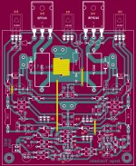
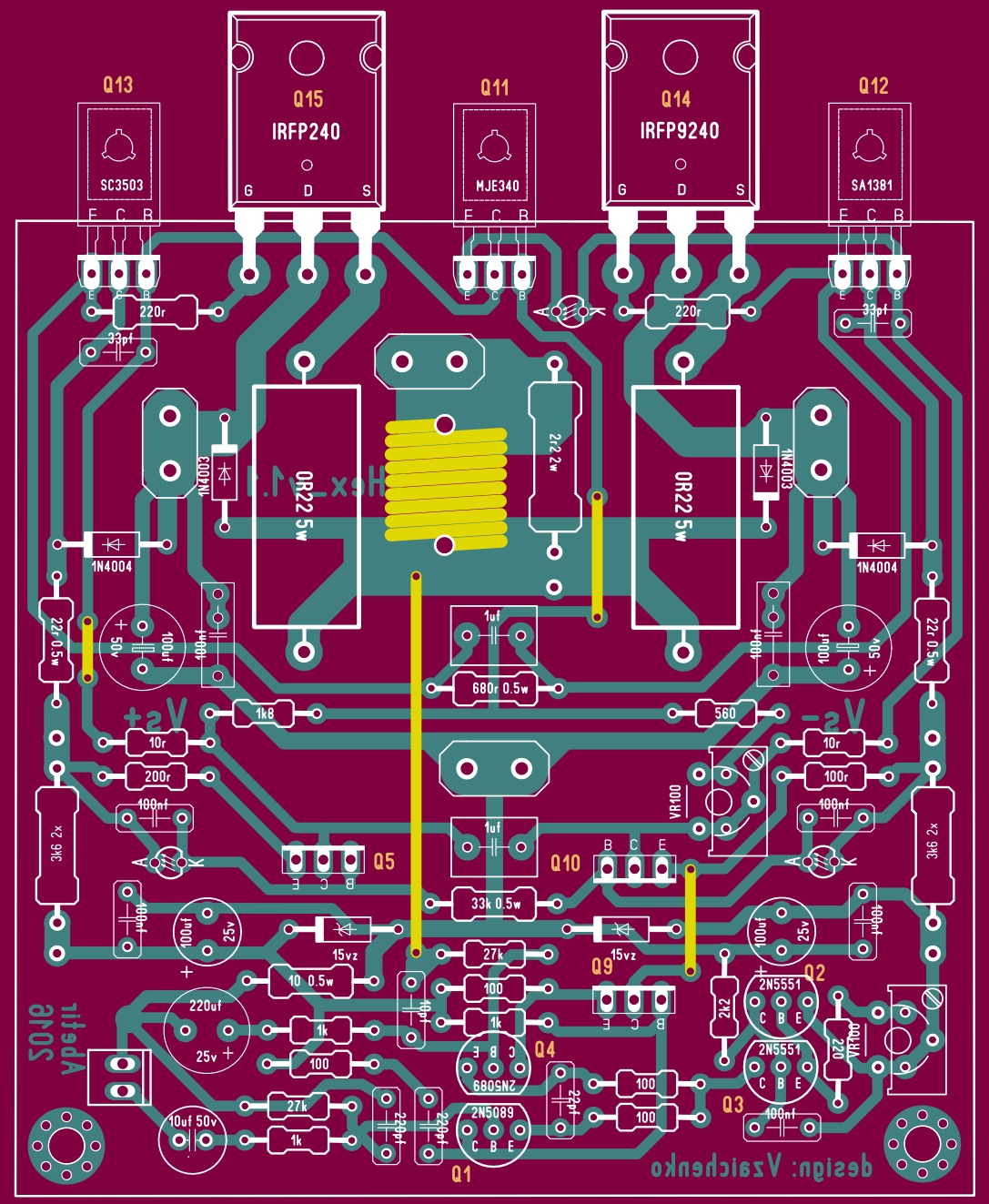
Ahha, found it - see this layout, made by Albert (excellent for the purpose, I think):
VHex 1.1 layout
Cheers,
Valery
Attachments
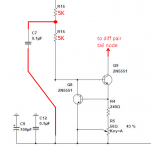
I prefer to move C7 "upstream". That way it doesn't wreck the high frequency performance of the Q8-9 negative feedback loop. The AC output impedance vs frequency of the current source (Q9) is also, in my opinion, quite a bit better when C7 is removed from the collector of Q8.
_
_
Attachments
Hi Mark,
Yes - valid point. Well, practical influence on overall performance will be not that high, but this is a good way of decoupling within such a feedback pair arrangement
Cheers,
Valery
Yes - valid point. Well, practical influence on overall performance will be not that high, but this is a good way of decoupling within such a feedback pair arrangement
Cheers,
Valery
Valery, can you post or provide a link to a the VHex 1.1 schematic so we can see what needs to be changed on abetir's board in order to use the circuit you posted in post number 126?
Thanks.
Thanks.
Valery, can you post or provide a link to a the VHex 1.1 schematic so we can see what needs to be changed on abetir's board in order to use the circuit you posted in post number 126?
Thanks.
Hi Ammel,
Here we go: VHex V1.1 schematic
There's also my version of the compact layout there, but I think the Albert's one is better, plus it's already tested.
Cheers,
Valery
Valery,
Thanks - this looks like a great option for an ultimate class A headamp/preamp. For 24v rails, what do I need to change as far as resistor values? Is there a Gerber file for this somewhere?
Thanks,
X
Thanks - this looks like a great option for an ultimate class A headamp/preamp. For 24v rails, what do I need to change as far as resistor values? Is there a Gerber file for this somewhere?
Thanks,
X
Valery,
Thanks - this looks like a great option for an ultimate class A headamp/preamp. For 24v rails, what do I need to change as far as resistor values? Is there a Gerber file for this somewhere?
Thanks,
X
Let me redraw V1.1 with all the amendments - it will be easier, leaving less space for some error.
If you can ping Abetir in the meantime - he is a very nice guy and I'm sure he will help us to amend the layout - he's got the source files.
Hello everyone
I do not remember who the diagram (Clepsidra) but here following a linear preamplifier that works rather well.
If some are interested I can provide the files required for its implementation.
Regard's
Diagram made for Dr Bora (RIP). Version with tone control
Attachments
Dear Valery, don´t know what are you simulating , what data are you feeding the software, but let´s see the actual schematic block by block.Guys, in many cases, knowledgeable experienced people are posting their comments, based on either some "well known" general information, or some very rough assumptions.
You are just confusing the less experienced members, reading your comments and making decisions, based on the very rough, inaccurate information you provide.
Now, let's see what the truth is.
I'm talking about schematic from the post #7 (top picture - bjt input version, attached here as well for your reference).
OLG @ 1KHz = 80db (far from 30db, mentioned above)
THD @ 1KHz open loop = 0.03% (not bad at all for open loop with such gain)
ULGF = 1.8MHz
CLG @ 1KHz = 12db (as set by the FB network)
THD @ 1KHz = 0.00011% (not enough for somebody?)
Output impedance = 9.7 ohm (more than "low enough" for driving some 10...100 Kohm input impedance of the power amp). Don't forget - NFB reduces the output impedance.
Conclusion - perfect for the purpose.
Please ... let's try to keep more attention to detail.
Cheers,
Valery
You have 2 gain blocks there, and total open loop gain is the product of both gain ratios.
Let´s start by the second block, because it loads the first one and affects its gain.
I bet you simulate very high gain there because you consider the BC560C a common emitter amplifier, with a constant current (VERY high impedance) load .
That the constant current load is being modulated out of phase only increases gain.
Hey, so far it looks I´m agreeing with your results 🙂
Problem is, that "very high impedance load" is in parallel with a low value resistor. Did you consider that?
Will it affect stage gain?
You bet.
Where is the resistor to ground loading second gain stage?
NFB resistors 3k+1k=4k total.
What is second stage open loop gain? (considering no external load applied)
To begin with, those transistors are passing roughly 7mA so intrinsic emitter resistance is about 4 ohms, which must be added to emitter resistance 82 ohms.
So that stage gain is about 4k/86 ohms , some 46X or 33dB
Do you follow me so far?
If you do, we´ll continue analyzing the differential first gain stage .
Thanks.
NOTE: I am not considering (yet) the NFB net an NFB net but simply a couple resistors, connected from output to ground ... which they are, of course.
Nor will I remove them from tne circuit (what maybe your simulator is doing) because, hey ! , they are there !!
And they do load the output!
I ran across this in the Pass F5 Headamp thread.
Looks like fun. Might be a great preamp. I would add some RF suppression on the input.
Looks like fun. Might be a great preamp. I would add some RF suppression on the input.
- Home
- Source & Line
- Analog Line Level
- Transistor Preamp