Hi XRK971
Respect - nice project !!
i am interested , but i am just able to solder SMD but no chip (no hot gun).
maybe an other option - my proposal:
pcb bare
pcb with smd chips (3255, opamp..)
pcb with all smd
complete board
Qeustion:
#post 1 you wrote:
We are also mounting the main TPA3255 chip on the bottom side so that its thermal pad faces down towards the mounting surface. In this way, the board just needs to be mounted to a metal chassis with the usual standoffs and a small thermal conductor block (aluminum or copper) can be used to mount this amp inside a sealed (non-ventilated) chassis, yet still permit adequate cooling.
i am afraid about the exact aligment of this metal plate because of the exact distance of the spacers - otherwise the chip will cracked. how do you handle this?
thanks
chris
Thanks! Good idea about having just TPA3255 and opamps pre-soldered - I’ll see what I can do. I can do a few of them by hand with paste and hot air.
Regarding mounting the heatsink block - use the thick blue silicone thermal pads (circa 1.5mm thick), they have lots of compliance. There are two bolt holes next to the chip, standoffs could be used to make sure it doesn’t compress further than stand-off height.
Regarding mounting the heatsink block - use the thick blue silicone thermal pads (circa 1.5mm thick), they have lots of compliance. There are two bolt holes next to the chip, standoffs could be used to make sure it doesn’t compress further than stand-off height.
My post #4 asked similar question so if there is the option to supply SMD populated or atleast the 'chips' then I would be interested.
Cheers
Cheers
According to the datasheet, the thermal "Powerpad" should require no more than a 10mm x 5mm heat transfer area if a thermal conductor were to be used. Something like 20mm x 10mm thick bar stock, cut to say, 10mm sections should work well. The chip itself has 1.2mm height, this plus 10.0mm thick thermal block gives 0.8mm gap for a silicone gasket. Two 0.5mm thick silicone silicone sheets, plus block should give 0.2mm compliance required if using a 12.0mm standoff.
Copper bar stock 20mm x 10mm thick x 100mm long:
COPPER FLAT BAR - 10mm x 20mm - 100mm LONG - NEW HIGH QUALITY | eBay
0.5mm silicone thermal pad:
Thermal Conductive Silicone 100x100mm x 0.5mm GPU CPU Heatsink Cooling Pad Blue 6914532858883 | eBay
Copper bar stock 20mm x 10mm thick x 100mm long:
COPPER FLAT BAR - 10mm x 20mm - 100mm LONG - NEW HIGH QUALITY | eBay
0.5mm silicone thermal pad:
Thermal Conductive Silicone 100x100mm x 0.5mm GPU CPU Heatsink Cooling Pad Blue 6914532858883 | eBay
Attachments

Doing so wouldn't allow to run the 3255 at full power continiously. The silicone spacer most likely do not provide low enough thermal impedance.
Quote from TI support for further calculations:
This is especially important when using the amp in BTL/PBTL at low frequencies. Just keep in mind, that the effciency is at around 90% at full power. So still 60W of power that needs to be dissipated somewhere. Even when taking crest factor into account, the burst capability is limited by the thermal impedance. So even if your heatsink is capable of dissipating the power, with a high impedance link/interconnection, it won't work.
Quote from TI support for further calculations:
The run the 3251 or 3255 at full power cont. the thermal connection needs to be low impedance. (Using no thermal pad together with minimal thermal grease and a milled down/polished thermal sink/heatsink).For the thermal calculation, TPA3251 data sheet gives ThetaJC=0.2 C/W, but if I look at silicon+die attach stack, I get a different number. Mine is a very crude 1D model, so it is very unofficial (don't quote this as a TI number). We really need to do 2-D computer analysis of the total thermal stack for true accuracy. Still, as a napkin calculation you can start with this:
Silicon thickness: 0.4mmSilicon conductivity: 0.117 W/mmK
heat conducting area: ~15mm^2 (assuming mostly from powerFETs)
Silicon: Theta J-DA= 0.23 degC/W
Die attach thickness: 0.05mm
Die Attach conductivity: 0.006 W/mmK
Die attach area ~25 mm^2
Die attach to Case: Theta DA-Case= 0.33 degC/W
Total Theta JC = 0.23+0.33= 0.56 degC/W
Copper heat pad thermal resistance should be negligible, but it needs to help spread the heat from ai internal die attach area of ~25mm^2 to a total external pad area of 48mm^2 (12mm x 4mm). You may wish to use an effective area somewhere between 25 and 48mm^2 to calculate your heat sink grease thermal resistance.
As a bench experiment, to calibrate thermal assumptions we sometimes use the OTW warning to help read the internal die temperature of 125C at different power dissipation levels/heat sink combinations. You also need to know (total power in) - (total power out) to know the dissipation.
This is especially important when using the amp in BTL/PBTL at low frequencies. Just keep in mind, that the effciency is at around 90% at full power. So still 60W of power that needs to be dissipated somewhere. Even when taking crest factor into account, the burst capability is limited by the thermal impedance. So even if your heatsink is capable of dissipating the power, with a high impedance link/interconnection, it won't work.
Last edited:
If you are going to run full power, any typical passive fin heatsink attached to the pad is not enough. Even the nice looking splayed out radial fin one by 3e. That looks like it is good for 10W to 15W dissipation max. Assuming 90% efficiency, then that's 150w max continuous RMS out of the amp into the speakers.
I suppose the other option is to use higher quality Keratherm pads. If anyone wants to run 400w rms continuous, they will need to remove 40w. A TO-247 MOSFET with a silicone pad is routinely used on Class A power amp at 35w to 40w. When I run an amp with 150w dissipation (per MOSFET), I use ceramic pads with thermal paste and fan cooled CPU coolers.
I don't think this is a real issue for most DIY'ers here. Also, it has auto-thermal protect in any event.
So, even if the chip were facing up, you would still have issues mounting your big-enough heatsink to it. Probably a fan cooled heat pipe CPU cooler type would be needed.
No 2d thermal model is needed if we prior experience with properly cooling much higher wattage and heat flux Class A amps.
Here is example of a ceramic insulator pad and CPU cooler with fan running happily with 150w dissipation (per fan):
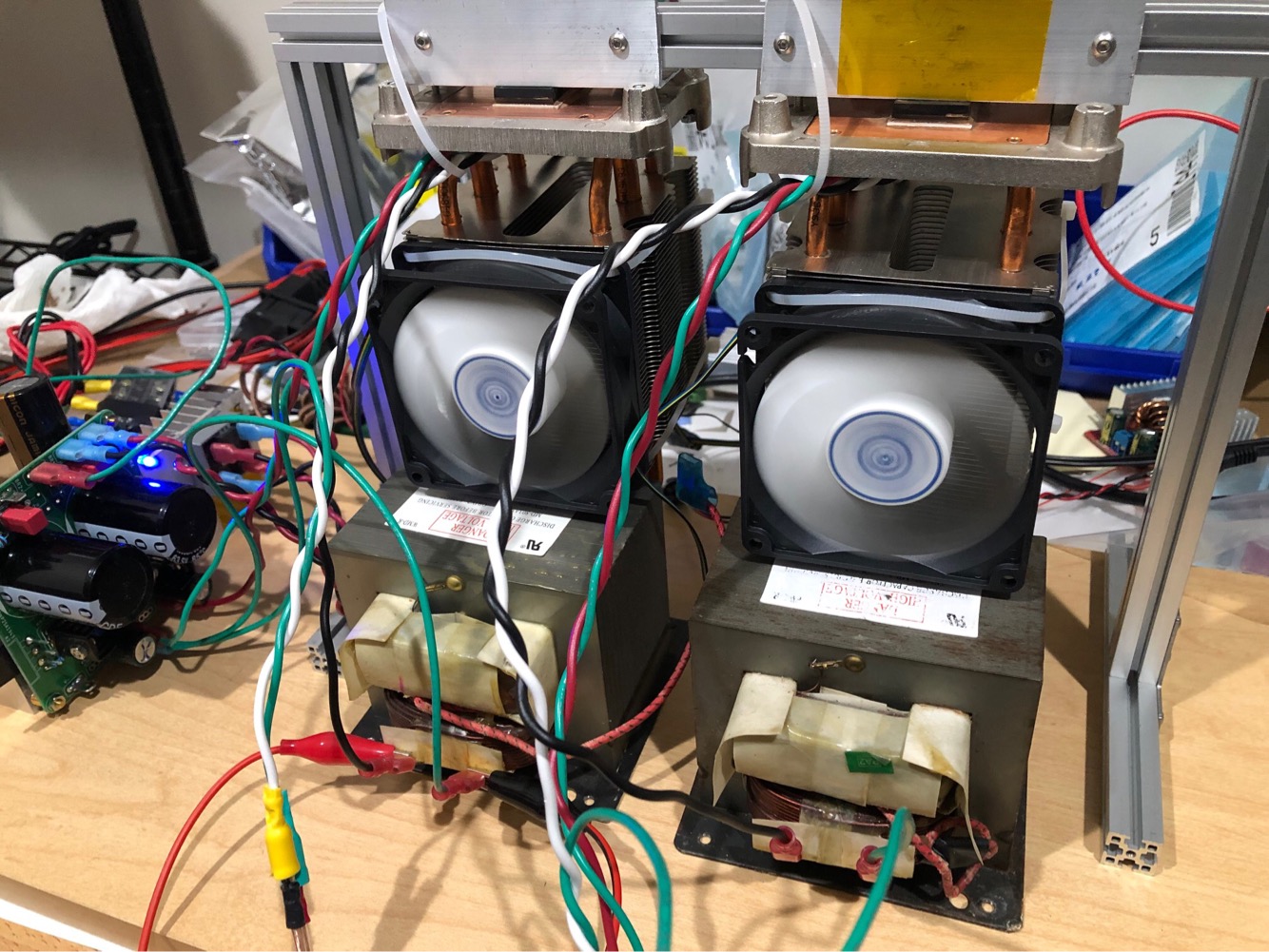
Here is about 100w per fan:
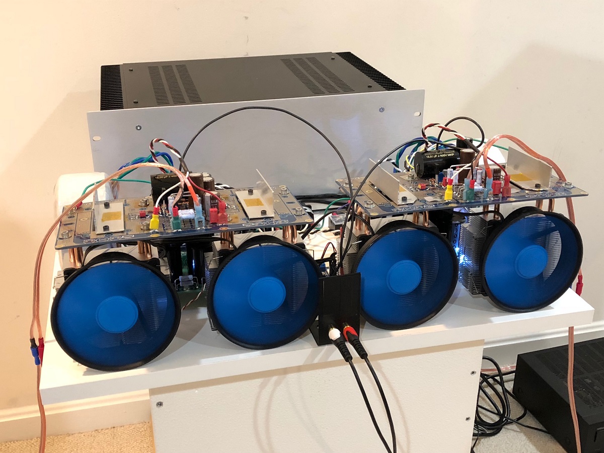
Countless examples of 35w per TO-247 MOSFET with silicone spacers and heatsinks can be found in the Pass Class A amp forum. Basically, cooling that TPA3255 PowerPad at extreme power levels is possible and it's a non-issue since we know how to deal with it.
I suppose the other option is to use higher quality Keratherm pads. If anyone wants to run 400w rms continuous, they will need to remove 40w. A TO-247 MOSFET with a silicone pad is routinely used on Class A power amp at 35w to 40w. When I run an amp with 150w dissipation (per MOSFET), I use ceramic pads with thermal paste and fan cooled CPU coolers.
I don't think this is a real issue for most DIY'ers here. Also, it has auto-thermal protect in any event.
So, even if the chip were facing up, you would still have issues mounting your big-enough heatsink to it. Probably a fan cooled heat pipe CPU cooler type would be needed.
No 2d thermal model is needed if we prior experience with properly cooling much higher wattage and heat flux Class A amps.
Here is example of a ceramic insulator pad and CPU cooler with fan running happily with 150w dissipation (per fan):
Here is about 100w per fan:
Countless examples of 35w per TO-247 MOSFET with silicone spacers and heatsinks can be found in the Pass Class A amp forum. Basically, cooling that TPA3255 PowerPad at extreme power levels is possible and it's a non-issue since we know how to deal with it.
Last edited:
Sure, if silicon+die attach stack is the same. (Beside the fact that the powerpad is smaller than on a TO-247 case).
Doesn't the powerpad require a good electrical connection to the ground plane through the heatsink meaning you can't use a silicon pad between them? Also it looks like the heatsink isn't currently connected to ground at all by the standoffs.
Maybe just use a metal block, 1-1.2mm washers to standoff the block with just thermal grease as the interface and in turn mount this to the chassis with an electrical insulator (Else it'll mess up your star ground!).
My other concern is the use of a really handsoldering unfriendly component (N131: LM5010ASD/NOPB) which is then totally surrounded with other components, just looks like a soldering nightmare to me!
The reset supervisor (N211: TPS3802K33DCKR) is also a 0.65mm pitch component! I respect you want to keep closely to the reference design but there must be an alternative that isn't described by TI as an "Ultra-Small" component.
Just seems strange that you have changed all the resistors to 0805 parts minimum then kept these tiny components. The board layout generally looks like it has been designed with a pick and place rather than handsoldering in mind.
Please don't take this as criticism, I'm actually genuinely interested, just want to make sure I can actually assemble this!
Note T3: Heat sink needs to have a good connection to PCB ground.
Maybe just use a metal block, 1-1.2mm washers to standoff the block with just thermal grease as the interface and in turn mount this to the chassis with an electrical insulator (Else it'll mess up your star ground!).
My other concern is the use of a really handsoldering unfriendly component (N131: LM5010ASD/NOPB) which is then totally surrounded with other components, just looks like a soldering nightmare to me!
The reset supervisor (N211: TPS3802K33DCKR) is also a 0.65mm pitch component! I respect you want to keep closely to the reference design but there must be an alternative that isn't described by TI as an "Ultra-Small" component.
Just seems strange that you have changed all the resistors to 0805 parts minimum then kept these tiny components. The board layout generally looks like it has been designed with a pick and place rather than handsoldering in mind.
Please don't take this as criticism, I'm actually genuinely interested, just want to make sure I can actually assemble this!
Fyrbird,
Thanks for the reminder about heatsink ground. Will see if we can use stand-off bolt then. Regarding parts soldering. This was made with paste solder in mind. You can’t hand solder some of this and paste with hand placed parts is so much easier than solder iron / and neater too. If you don’t have a $40 hot air pencil. Use a $10 hot plate and old skillet. YouTube how to videos abound on this. Check them out. You won’t ever go back to hand soldering with an iron.
Thanks for the reminder about heatsink ground. Will see if we can use stand-off bolt then. Regarding parts soldering. This was made with paste solder in mind. You can’t hand solder some of this and paste with hand placed parts is so much easier than solder iron / and neater too. If you don’t have a $40 hot air pencil. Use a $10 hot plate and old skillet. YouTube how to videos abound on this. Check them out. You won’t ever go back to hand soldering with an iron.
I’d recommend the MIC8114 supervisor, which is more robust to glitches and has longer minimum reset time. (And it is more handsolder-friendly + cheaper)
That’s up to you, many people like a linear toroidal supply but that requires a bridge rectifier and smoothing caps and it’s quite heavy. They are very reliable though. I have not tested a TPA3255 with a linear yet although I should. I have used an 800w 48v SMPS from Connexelectronic and it provides the juice but I can hear hiss on the speaker output with my ear 2-3in from speaker. When I switched to a 12v 35Ahr gel cell deep cycle battery (for a UPS), with a 600w step up DC-DC and running at 52v - the output was dead silent. The sound was very good too - I feel a battery gives great current reserves, even when powered through a DC-DC step up. With my Fluke 101, I measured 0.1mV to 0.0mV rms. A very good result for any large power amp.
The battery was able to power the amp +24hrs at usual listening levels in the home. Calculations show that playing 120wrms will last about 5hrs. You can attach a small 1A trickle wall charger to top off when not in use. The battery setup is less expensive than the 800w Connexelectronic PSU.
The battery was able to power the amp +24hrs at usual listening levels in the home. Calculations show that playing 120wrms will last about 5hrs. You can attach a small 1A trickle wall charger to top off when not in use. The battery setup is less expensive than the 800w Connexelectronic PSU.
Well actually I need only 100-120W per CH. So I will use about 40V and 7A. Or do you think that is better use higher voltage and lower current?
Here is how I would go about spec'ing the PSU:
120wrms into 8ohms requires 88 Vpp or 31 Vrms. Assuming sine wave signals, using P=IV, we can calculate RMS current as 3.87A, but with capability to reach 11A peaks. In BTL mode, the maximum output voltage is double the Vdd, or Vdd needs to be 44V. I would give it some margin like extra 2 V or 46 V rated at 4A continuous, and capable of momentary output out to 11A.
120wrms into 8ohms requires 88 Vpp or 31 Vrms. Assuming sine wave signals, using P=IV, we can calculate RMS current as 3.87A, but with capability to reach 11A peaks. In BTL mode, the maximum output voltage is double the Vdd, or Vdd needs to be 44V. I would give it some margin like extra 2 V or 46 V rated at 4A continuous, and capable of momentary output out to 11A.
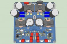
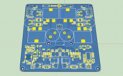
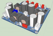
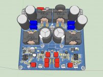
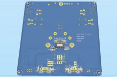
JPS64 just finished all the updates listed below. Thank you to all the folks who gave feedback on the layout and design. I think it’s going to be a killer amp.
Here is a summary of the changes:
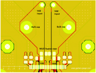
1. Larger low impedance paths for Vdd from power supply input to pins on IC with good connection to bulk caps.
2. Move inductors apart to prevent magnetic cross talk that can increase distortion.
3. Add PFFB option.
4. Add 2k2 and 220pF input RFI filter.
5. Add ground pad on heatsink mounting hole for conductive standoff to ground the heatsink to 0v (but still insulate from chassis ground).
6. Change to MIC8114 shutdown supervisor.
3D renders below along with schematics. Board is 2-layer 120mm x 120mm x 2mm thick with 2oz copper and ENIG.
Thank you to JPS64 for another masterpiece. Truly amazing work for the DIY community!
Here is a summary of the changes:
1. Larger low impedance paths for Vdd from power supply input to pins on IC with good connection to bulk caps.
2. Move inductors apart to prevent magnetic cross talk that can increase distortion.
3. Add PFFB option.
4. Add 2k2 and 220pF input RFI filter.
5. Add ground pad on heatsink mounting hole for conductive standoff to ground the heatsink to 0v (but still insulate from chassis ground).
6. Change to MIC8114 shutdown supervisor.
3D renders below along with schematics. Board is 2-layer 120mm x 120mm x 2mm thick with 2oz copper and ENIG.
Thank you to JPS64 for another masterpiece. Truly amazing work for the DIY community!
Attachments
Last edited:
- Home
- Group Buys
- TPA3255 Reference Design Class D Amp GB