According to the data sheet: "TPA3255 achieves both high power efficiency and very low power stage idle losses below 2.5W."
But you have also DC/DC converter and LDOs.
But you have also DC/DC converter and LDOs.
Waiting on R1021-1024 and r101,102,111,112. Still being punished for using that BOM on page 11 🙂
I asked a mod to edit that post and point to the latest BOM for v002p. Sorry about that!
Typo is 0.047uF 100v X7R 1206 should be 0.01uF 100v 1206 X7R. Please use this cap for C133, C261-264:
VJ1206Y103KBBBE31 Vishay / Vitramon | Mouser
For R1021 to R1024, use anything from 10R to 220R. I have found 51R to be a good compromise.
So, just to confirm, the May 7th BOM (Post #503) is still incorrect for C133, C261-264, correct?
Thanks,
Pete
The BOM states the correct specification of 0.01uF 100v X7R 1206, but the part number linked is an 0.047uF cap. So please make sure you use the updated note for the 0.01uF part.
At some point I need to update a final BOM with no more errors and also tell people to disregard all other previous BOMs.
I am not certain we have caught 100% of them yet. Note that if you are getting the non-PFFB version 001 board (blue), you don’t need parts R_A/B/C/D.
I appreciate folks sending me notices when they find an error or discrepancy.
Someone has asked the right way to attach a single ended signal such as coming from an RCA to a balanced input buffer. The buffer itself adheres to the XLR convention which is pin 2 to +xe in, pin 3 to -xe in, and pin 1 to chassis. If you are connecting a single ended signal the signal + connects to pin 2, and the signal - connects to pin 3. It is highly recommended that signal - be isolated from chassis.
For those of you that are using two wire plus shield cabling with an RCA at the source end do it per Neurochrome's recommendation, which is to connect the RCA center pin to the wire comprising +xe and the RCA outside to both -xe and shield at the source end. At the buffer input connect the +xe wire to pin 2, the -xe wire to pin 3 and the shield to pin 1.
When will you pcb be available please? Looks like I will need a buffer.
I just got the revised design for the verification build BTSB Buffer today. Will order boards now. However, if you are interested in the prototype version I can get you that. It has a pad error on XLR jack. Doesn’t fit perfectly. But if not using it then it’s fine.

Great news Nrabbit! That's two others who have built this amp besides me and gotten it to work! Be careful using it on carpet like that - static discharge.
I just got the revised design for the verification build BTSB Buffer today. Will order boards now. However, if you are interested in the prototype version I can get you that. It has a pad error on XLR jack. Doesn’t fit perfectly. But if not using it then it’s fine.
Thanks X. I am going to use the onboard XLRs. How bad is the misalignment? Is it the mounting pins or the signal pins?
You have to bend the larger pins by 1mm not much. It still works and is quite secure as there are line 8 pins soldered. Both Redjr and I are doing it and ok with it. Just doesn’t look perfect.
As you can see, here is Redjr’s build:
The new board I have actually has SE output in addition to the balanced but the XLR pins are still off.
As you can see, here is Redjr’s build:
The new board I have actually has SE output in addition to the balanced but the XLR pins are still off.
Last edited:
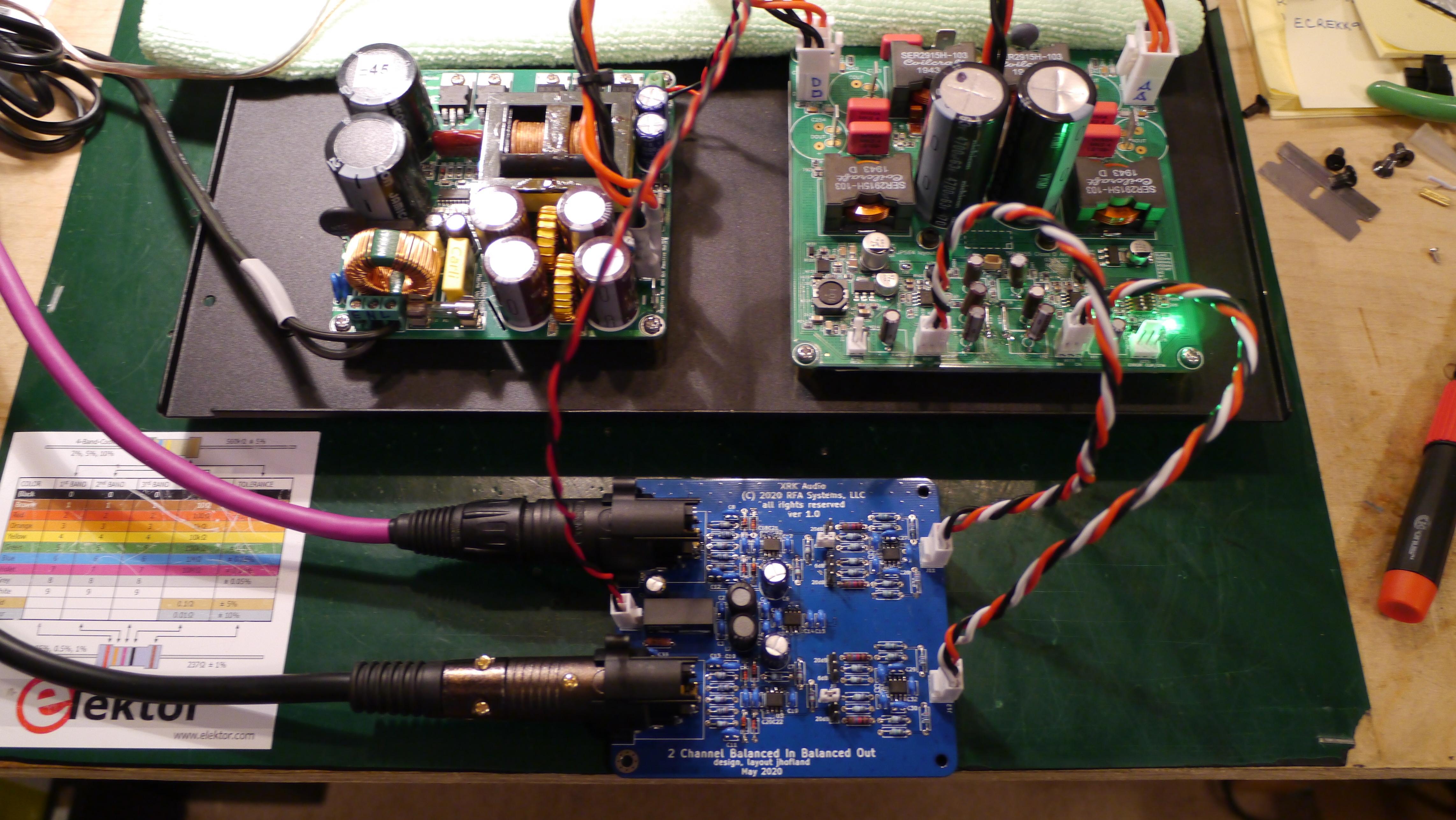
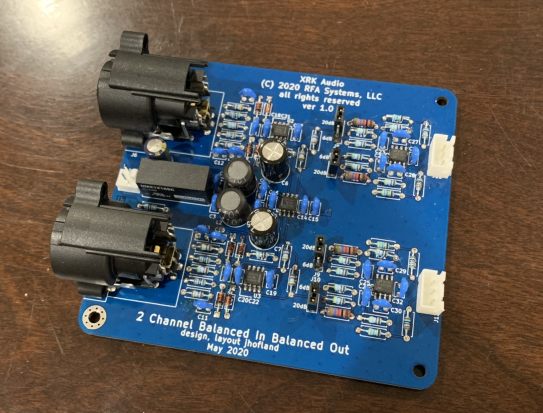
Prototype SE/Bal to Bal converter by jhofland for driving the TPA3255:
Just got done assembling. Will test later.
Count me out
Looks very original though...
Sure you have all the research to back up that design.
Where's Apex been lately?
Nothing for you to remix from him so here we are.
You went from that power supply to brilliance?!? 🙄
Driving the offset with an OPA1656??
That's one for the books.
You made a go at TMC.
How's your Etsy shop going?
Last edited:
Hi 808,
Do I know you? Because you speak a little too familiar and I have no idea what you are talking about.
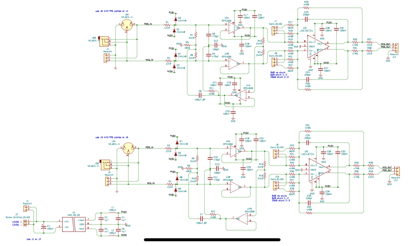
Not sure what kind of research you are talking about to back what up? This is a design by jhofland, a seasoned designer with 50yrs+ of experience. The middle OPA1656 provides a bootstrap for the two input stage OPA1656’s. Not for offset.
What’s TMC?
Do I know you? Because you speak a little too familiar and I have no idea what you are talking about.
Not sure what kind of research you are talking about to back what up? This is a design by jhofland, a seasoned designer with 50yrs+ of experience. The middle OPA1656 provides a bootstrap for the two input stage OPA1656’s. Not for offset.
What’s TMC?
You have to bend the larger pins by 1mm not much. It still works and is quite secure as there are line 8 pins soldered. Both Redjr and I are doing it and ok with it. Just doesn’t look perfect.
As you can see, here is Redjr’s build:
The new board I have actually has SE output in addition to the balanced but the XLR pins are still off.
Ok happy to take an original board then thanks.
Just for clarification... I had to snip 2 of the leads that went to the inner sleeve of the jack - used for the TRS - to get it to seat properly on the PCB. Otherwise, there would have been obvious stress on both the jack and the PCB that I didn't like. Just couldn't bend those 2 pins into place. I have no intention of ever using the 1/4" part of this combi-XLR jack. If I did/use more with 1/4" balanced jacks/plugs, I may have made another decision. My OCB lost this time. 🙂Ok happy to take an original board then thanks.
I'm currently waiting on my case panels from FPE to get here. I'll have some pictures to share of my finished map in a couple weeks.
Don't take it personally, if you read this thread you'll understand.Hi 808,
Do I know you? Because you speak a little too familiar and I have no idea what you are talking about.
Fully Differential Headphone Amplifier
For freq_adj, are the resistors run in parallel? (for example, 500khz would be dip 5 + 6 ON?)
Not frequency adjustment but gain adjustment.
Here is the latest schematic of the BTSB Buffer. The gain resistor DIP switch is in parallel, however, individual ones (4-bits) provide 0dB, 6dB, 14dB, and 20dB. Certain parallel combinations of the above could produce finer scale changes by making the input resistor smaller via parallel equivalent.
Layout:
Let me start a new GB thread for it.
Attachments
Last edited:
Err.. I meant on the tpa3255. For freq_adj, are the resistors run in parallel? (for example, 500khz would be dip 5 + 6 ON?)
You need to read the data sheet, it follows whatever TI setup. It doesn’t work like that. I think the resistors set a voltage that is used by an ADC to read a preset fixed frequency.
- Home
- Group Buys
- TPA3255 Reference Design Class D Amp GB