I have a few questions on these newer TI class-D chips...
(1) Are the 3250 and 3251 the exact same circuit, differing only by thermal pad placement? (I understand this is the case for the older 3116 and 3118 chips.) If they are the same, why is it that the performance graphs in the datasheets for the 3250 and 3251 are different? Looks like 3251 is ever-so-slightly better.
(2) Operating in stereo BTL mode, the 3251 requires balanced inputs. If the source is unbalanced, what is the "best" way to feed the 3251 its balanced signal? I.e., convert on the amp board itself (like I've seen many in this thread do), or convert as close to the source as possible? I know better than to ask "what's best" on this forum") , so what I really mean is, what considerations might one take into account when weighing one approach over the other? In my naive mind, it seems you'd want to convert as close to the source as possible (e.g. using something like this), so you get the benefit of differential signaling over the length of the cabling.
, so what I really mean is, what considerations might one take into account when weighing one approach over the other? In my naive mind, it seems you'd want to convert as close to the source as possible (e.g. using something like this), so you get the benefit of differential signaling over the length of the cabling.
(3) There has been some discussion in this thread about how short the tpa3251 IC is, making it hard to get a small/tight PCB layout without a custom heatsink. Would it make any sense to create a "shim" for the chip, just to create some clearance for surrounding components? What I'm thinking is a PCB that's basically just big enough for the tpa3251 IC, and bordered by plated holes that correspond to the chip's pins. The actual PCB (with all the supporting components/circuitry/input/output), would have matching plated holes. Then you could just mate the "shim" to the actual PCB, and that should create enough clearance for all the components you want to be really close to the chip. Or maybe instead of plated holes you create an actual pin array + socket (kind of like an RPi hat). Obviously this idea still adds distance between the chip and components, but it's a little vertical distance versus greater horizontal distance. Maybe not enough to matter? Or maybe it's actually worse because you're adding junctions instead of a straight trace? Dunno, that's why I'm asking.
(4) Anyone with working 325x amps care to comment on their experience? Given the volume of attention the tpa311x chips got, I'm surprised these newer chips haven't taken off in similar fashion. Going just by the datasheets, they look substantially better.
(1) Are the 3250 and 3251 the exact same circuit, differing only by thermal pad placement? (I understand this is the case for the older 3116 and 3118 chips.) If they are the same, why is it that the performance graphs in the datasheets for the 3250 and 3251 are different? Looks like 3251 is ever-so-slightly better.
(2) Operating in stereo BTL mode, the 3251 requires balanced inputs. If the source is unbalanced, what is the "best" way to feed the 3251 its balanced signal? I.e., convert on the amp board itself (like I've seen many in this thread do), or convert as close to the source as possible? I know better than to ask "what's best" on this forum
, so what I really mean is, what considerations might one take into account when weighing one approach over the other? In my naive mind, it seems you'd want to convert as close to the source as possible (e.g. using something like this), so you get the benefit of differential signaling over the length of the cabling.(3) There has been some discussion in this thread about how short the tpa3251 IC is, making it hard to get a small/tight PCB layout without a custom heatsink. Would it make any sense to create a "shim" for the chip, just to create some clearance for surrounding components? What I'm thinking is a PCB that's basically just big enough for the tpa3251 IC, and bordered by plated holes that correspond to the chip's pins. The actual PCB (with all the supporting components/circuitry/input/output), would have matching plated holes. Then you could just mate the "shim" to the actual PCB, and that should create enough clearance for all the components you want to be really close to the chip. Or maybe instead of plated holes you create an actual pin array + socket (kind of like an RPi hat). Obviously this idea still adds distance between the chip and components, but it's a little vertical distance versus greater horizontal distance. Maybe not enough to matter? Or maybe it's actually worse because you're adding junctions instead of a straight trace? Dunno, that's why I'm asking.
(4) Anyone with working 325x amps care to comment on their experience? Given the volume of attention the tpa311x chips got, I'm surprised these newer chips haven't taken off in similar fashion. Going just by the datasheets, they look substantially better.
1. Yes, but output stage FET-size might differ.
2. convert on ampboard itself or use a line-driver/receiver.
3. a small copper shim on top of the IC is sufficient, no need to do an extra PCB. Some parts are critical and need to get placed as close as possible to the chip. Any millimeter adds up unnecessary parasitic effects to the circuit. Best would be to mount the IC "trough" the board like hanging upside-down to the opposite side of the pcb and the bold every on a heatsink.
Btw. You can order the custom made EVM heatsink at digi-key.
It surprises me too. When the specs of this chip, esp. THD + N and power, are an order of magnitude better than those of 311x chips, why are the 325x chips not getting that much attention.
Is it because of price? The 3116D2 board costs less than $10, whereas the 3251 board costs $90 on eBay.
Is it because of price? The 3116D2 board costs less than $10, whereas the 3251 board costs $90 on eBay.
Is it because of price? The 3116D2 board costs less than $10, whereas the 3251 board costs $90 on eBay.
The 3116 series of parts are very easy to implement and are virtually stand alone. The 325x parts need many support ICs to form a flexible and fully functional amplifier. They also require more components too.
TI could release a stand alone 325x part but it'd probably have slightly lower performance and most likely be voltage limited. That said I don't think anyone would mind a lower power version of the 3251, with onboard regulator, and analogue front end that could accept SE inputs.
Waiting for Yatsushiro''s comparison of 3251 with other boards' performance ...
Getting my house in England ready to sell before i move to France means this won't happen for a few months yet...
Getting my house in England ready to sell before i move to France means this won't happen for a few months yet...
Oh! It's OK.
And best of luck. You have a huge task on your hands.
Please try and tell me how it is.
Or look here:
TPA3251 (TPA3255) Stereo Verstarker Amplifier Mini 2x175W (2x140W) | eBay
TPA3251 (TPA3255) Stereo Verstarker Amplifier Mini 2x175W (2x140W) | eBay
Or look here:
TPA3251 (TPA3255) Stereo Verstarker Amplifier Mini 2x175W (2x140W) | eBay
TPA3251 (TPA3255) Stereo Verstarker Amplifier Mini 2x175W (2x140W) | eBay
I have a TPA3251D2EVM board that I'm sorting for a friend. I upgraded the op-amps to lme49720's and started testing with resistive loads for max power before clip LED illumination. The results somewhat lower than I anticipated for 1kHz @ 36V:
51W into 8 Ohm
95W into 4 ohm
123.5W into 2 ohm
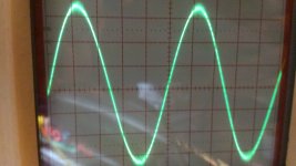
I get 72W and 138W into 8 ohm and 4 ohm respectively before flat top clipping which is in line with the 1% THD+N figures in the datasheet. The waveforms however look far worse than 1% THD+N with a lot of switching noise, see attached.
There is also 1.2V pk-pk at ~570kHz imposed on the output signal at all times, irrespective of power output.
Does any of this seem familiar to anyone?
Thanks
51W into 8 Ohm
95W into 4 ohm
123.5W into 2 ohm
I get 72W and 138W into 8 ohm and 4 ohm respectively before flat top clipping which is in line with the 1% THD+N figures in the datasheet. The waveforms however look far worse than 1% THD+N with a lot of switching noise, see attached.
There is also 1.2V pk-pk at ~570kHz imposed on the output signal at all times, irrespective of power output.
Does any of this seem familiar to anyone?
Thanks
Attachments
Last edited:
I saw some discussion about inductors here.
What I typically do, is to take the maximum peak current at 1% at take that as a value for the inductor.
So 200Wrms @ 4ohm would be around 10A peak.
Take the point where the current is just getting lower (like the knee).
That way you know that you have at least some room to play.
Btw, another great, good performing and very affordable brand is Sumida.
The question I have;
The input voltage in the datasheets, is that the differential voltage or single ended voltage?
Any commercial supplier available for 10uH air core inductors with low DCR-loss and 15A current rating which aren't huge in size?
Sumida CDEP147NP series are very close to that?
(and affordable as well)
Last edited:
You CANNOT judge THD by the scope plot of class-d outputs.The waveforms however look far worse than 1% THD+N with a lot of switching noise, see attached.
There is also 1.2V pk-pk at ~570kHz imposed on the output signal at all times, irrespective of power output.
Thanks
The visible "smearing" may vanish into zero after an appropriate low-pass filter.
Furthermore THD of a BTL-configuration should be measured across bridge outputs -
measuring between on half-bridge out and GND will show wrong results.
And finally: Yes, this is a switched amp and therefore you will find some RF residudual at the output on any class-d amp.
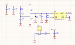
So I've built a TPA3251 board and got everything working except for the Voltage Supervisor circuit. Now, my implementation is a mix of the EVM versions with changes made based on info in this thread so maybe I've messed it up somehow. The error I get is that RESET stays low and only periodically goes high for a few microseconds and the fault LED flashing very briefly. I've measured VDD at the TPS3802 and it reads a constant 3.7V which seems fine (Note: R25 is 10k actual value). The header in the schematic is for manual reset with a jumper. To bypass the circuit I've just hardwired RESET to 3.3V which makes the amp work but isn't a very nice bodge
Thanks
Thanks
Attachments
Last edited:
Yes, I have probed both VDD and /RESET. VDD is stable while /RESET periodically goes high for a few microseconds. However, I found something during my measurements that makes it pretty clear why the circuit isn't working. When /RESET goes high the voltage on /MR goes down which starts an endless circle of resetting. So it seems like /MR gets bogged down by some load in the rest of the circuit when /RESET goes high. Tried decreasing the pullup resistor value on the /FAULT-line from 47k to 10k but no difference.
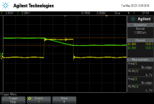
Attaching scope screenshot (channel 1 = /RESET, channel 2 = /MR) and the fault indicator circuit for completion.
/David
Attaching scope screenshot (channel 1 = /RESET, channel 2 = /MR) and the fault indicator circuit for completion.
/David
Attachments
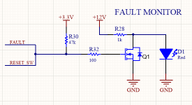
Something's really wrong here. /MR is pulled up to VDD internally by 30k. I can't think of anything in the chip which pulls down /MR as this is an input. May you plot a longer cycle? Please try also with removed R24.
Does the footprint pin numbers correctly relates to the schematic?
Does the footprint pin numbers correctly relates to the schematic?
Last edited:
- Home
- Amplifiers
- Class D
- TPA3251d2