Purpose every post regarding this was and will be, values do not matter when they are so far from chippins and silkscreen doesn't tell you values on YJ boards. Given the large distance I would favor danzz's order a little, but that is because I only listen to board 🙂
Purpose every post regarding this was and will be, values do not matter when they are so far from chippins and silkscreen doesn't tell you values on YJ boards. Given the large distance I would favor danzz's order a little, but that is because I only listen to board 🙂
I haven't argued that the values do matter here. I am not messing with those values.
Nor have I said anyone should replace values, or as I like, to put larger leaded caps instead. That's up to others to decide.
As I said, thanks for confirming the order the right and left side of IC that smd "should" be on this board.
Maybe you missed a recent contribution by sant_ka, he did recommend changing values, and I also did btw but main thing is distance of the first cap used, as in this sant_ka pic
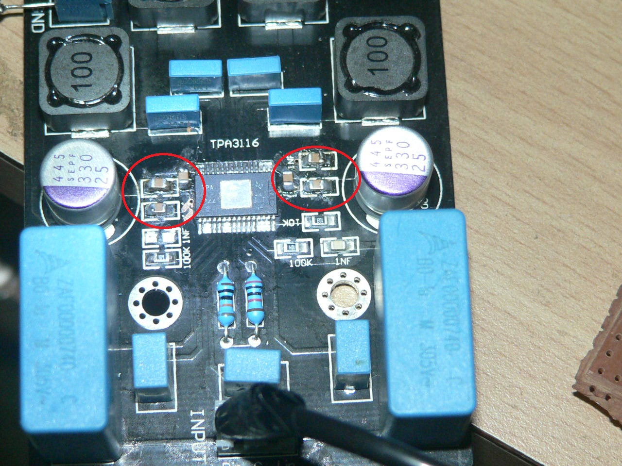
Maybe you missed a recent contribution by sant_ka, he did recommend changing values, and I also did btw but main thing is distance of the first cap used, as in this sant_ka pic
The 10nf on the data sheet is across power input right? Why not place it nearer to that, before the DC power electrolytic instead of between them and IC? Let's say on the underside for example!
Yes. Between PVCC and GND terminal on bottomside for example. It is conform datasheet, that is why I did it that way, also on other 3116's.
Yes. Between PVCC and GND terminal on bottomside for example. It is conform datasheet, that is why I did it that way, also on other 3116's.
I don't think I have seen pics of your 3116 board/s irribeo, and finding many things in this thread is sometimes pot luck.
That mod does make sense to me. Do you then leave the 10nf component out of the trace next to IC?
I don't think I have seen pics of your 3116 board/s irribeo, and finding many things in this thread is sometimes pot luck.
That mod does make sense to me. Do you then leave the 10nf component out of the trace next to IC?
For example I did like this:
DSCF3028_zpsma7tkabl.jpg Photo by snake69fast | Photobucket
I didn't remove the 1nF's or 10nF either
white smd=cog=100nF
yellow smd=classII XR=10uF(~5 or 6uF with voltage applied) but maybe 6uF will do fine too, TI used 0.1&1&22uF with some TAS chip, Wiener GB has another set of values
white smd=cog=100nF
yellow smd=classII XR=10uF(~5 or 6uF with voltage applied) but maybe 6uF will do fine too, TI used 0.1&1&22uF with some TAS chip, Wiener GB has another set of values
Last edited:
Can't be sure because of picture scale, but the boards I got have the smd a bit more symmetrically in-line with chip, and "look" slightly closer. In any case I don't think I could do that in that spot.
If the mod you show is done, is it vital to leave the original 10nf still in place?
I see that a small trace comes out under IC to it, presumably IC GND. But it also does at the 100nf at opposite end.
If the mod you show is done, is it vital to leave the original 10nf still in place?
I see that a small trace comes out under IC to it, presumably IC GND. But it also does at the 100nf at opposite end.
Yes your board might not be YJ, it isn't on yuanjingaudio website, which might be a good thing, but does mean you need to check traces, from photo it isn't really clear and what is visable is a little different, not same shape for traces. SMD pads seem little bigger and closer to chip, YJ has vias to gnd next to chip, can't see them on your. The distance from pvcc trace to first gnd-pad smd (10nF R-1nF L) seems maybe a little easier, at least for soldering 1 smd there. But you need to check gnd side is same, if they switched the smd's are close now. I think the 1nF's could still be in top place or a following place if you want them there.
Aye. Seller on eBay sold as "official YJ" boards, but I did get them cheap, and as slightly different to each other I did wonder. They both work, so that to me was a bonus.
Thought they were 2.0 versions on YJ website, that's what I was led to believe I was buying.
Anyhow. As I have switched 1nf, gonna have a go at switching the 10nf and 1nf around on the power input side to match other, and the order on datasheets i.e 1nf closest to pvcc pins.
As I'll be moving 10nf down the order I'll have a think about a second 10nf across pvcc/GND elsewhere before.
It does look like there's 2 small traces coming out from under IC from it GND pad to both the 10nf and 1nf on that side.
Time for some thought.
EDIT..... did the 10nf between pvcc and GND appear on the EVM board? Can't see it anywhere, but might be missing it.
Last edited:
I don't think YJblue changed, but components change all the time, silkscreen lettersize and place is identical on website to over 1 year ago. I haven't looked at TI evm recently and didn't even 🙂 buy a chinese "exact" copy that was around for some time. GMarsh Wiener GB has same functionality probably.
Its shocking how reading one small article shines light on tiny mistakes in circuitry!
Just read an old Creek audio piece on bypassing with Crescendo caps.... What struck me was the word "cascading" the bypass caps. It pointed out that my boards 1nf and 100nf smd pvcc bypass caps are not optimum.
I redrew the circuit, the nearest cap is paralleled with main power electrolytic, the second in the chain is in series with the first, which sort of parallels the power cap, but creates a small loop in circuit. And what's the point of two caps in series to bypass, especially with larger cap after smaller cap?
To put in another way.... If I redraw the existing circuit with the bypass traces overplayed with electrolytic circuit traces, the 2 smd bypass caps form a X (cross) over each other.
Wouldn't it be better to bridge the + of middle smd next to IC across to trace between power electrolytic and first bypass cap nearest first pvcc pins? This would put all 3 in parallel, remove the loop, and create a proper "cascading" high frequency bypass!
Am I along the right lines? Advice!
Last edited:
Its shocking how reading one small article shines light on tiny mistakes in circuitry!
Just read an old Creek audio piece on bypassing with Crescendo caps.... What struck me was the word "cascading" the bypass caps. It pointed out that my boards 1nf and 100nf smd pvcc bypass caps are not optimum.
I redrew the circuit, the nearest cap is paralleled with main power electrolytic, the second in the chain is in series with the first, which sort of parallels the power cap, but creates a small loop in circuit. And what's the point of two caps in series to bypass, especially with larger cap after smaller cap?
To put in another way.... If I redraw the existing circuit with the bypass traces overplayed with electrolytic circuit traces, the 2 smd bypass caps form a X (cross) over each other.
Wouldn't it be better to bridge the + of middle smd next to IC across to trace between power electrolytic and first bypass cap nearest first pvcc pins? This would put all 3 in parallel, remove the loop, and create a proper "cascading" high frequency bypass!
Am I along the right lines? Advice!
just took couple of pics to illustrate my post.
the first pic shows drawing of the board circuit as is.

the second pic shows two drawings....
The top drawing is the board circuit redrawn to show how the how the 2 smd bypass caps "X" (cross) each other, i.e the closest cap attached to the "+" pvcc trace returns to ground furthest away, and the furthest cap attached to pvcc "+" trace returns to ground nearest......surely this isnt optimum?
The Bottom drawing is my solution to the circuit loop created. By placing the 1nf nearest pvcc, and 100nf nearest electrolytic on poisitve traces and vice versa on negative return trace, it corrects a "cascading" bypass.

Creek audio had some very coloured classA (B) amps, they into class D these days ?
YJblue has stargnd at (under) 3116, your version too I thought you said, or did you mention already that layout pvcc/gnd for smd caps is reversed on your pcb ?
YJblue has stargnd at (under) 3116, your version too I thought you said, or did you mention already that layout pvcc/gnd for smd caps is reversed on your pcb ?
Creek audio had some very coloured classA (B) amps, they into class D these days ?
YJblue has stargnd at (under) 3116, your version too I thought you said, or did you mention already that layout pvcc/gnd for smd caps is reversed on your pcb ?
I recently bought what I thought was a YJ blue black from Amazon (listed as a HeroNeo) but it is different in that there is an LED and the bottom side has room for 3 SMT reverse polarity protection diodes, and the black paint on the bottom appears to have a cross-hatched silkscreen texture to it. The workmanship in general looks cleaner than my first YJ blue black. Is this the new version by YJ, or an improved knock-off of a knock-off of Danzz's board by yet another player? The parts are all blue (no white or yellow caps).
Amazon.com: HeroNeo® TPA3116D2 50Wx2 Official Version Finished Stereo Digital Power Amplifier Board: Electronics
Creek audio had some very coloured classA (B) amps, they into class D these days ?
YJblue has stargnd at (under) 3116, your version too I thought you said, or did you mention already that layout pvcc/gnd for smd caps is reversed on your pcb ?
I mentioned creek and the article to note the source of why I looked at this. I am not suggesting to copy their designs, but it did make sense looking at my board, and the 3116 schematic.
I think mine must have the star ground as no traces go from any IC gnd's, but as that isnt on data sheet schematics I don't really know much about that part of circuit, and definately not going to lift IC. But there is a trace coming out from under IC to the "bypass caps" positive trace, and returns to electrolytic negative on the 1nf/100nf side of board.
The drawings I posted are based on my board circuit and the 3116 schematic, the creek article had no drawings. The fact that the 1nf positive side is nearer to pvcc input than 100nf yet the opposite on return to electrolytic negative trace on board forms a "loop" in the circuit, and means both the 1nf and100nf does and doesn't bypass the electrolytic < that's difficult to explain, apart from the trace going from under IC to electrolytic. I also don't see any traces from the 100nf to under the IC.
I am more confused now!!!!! lol.
I recently bought what I thought was a YJ blue black from Amazon (listed as a HeroNeo) but it is different in that there is an LED and the bottom side has room for 3 SMT reverse polarity protection diodes, and the black paint on the bottom appears to have a cross-hatched silkscreen texture to it. The workmanship in general looks cleaner than my first YJ blue black. Is this the new version by YJ, or an improved knock-off of a knock-off of Danzz's board by yet another player? The parts are all blue (no white or yellow caps).
Amazon.com: HeroNeo® TPA3116D2 50Wx2 Official Version Finished Stereo Digital Power Amplifier Board: Electronics
That sounds like one of the boards I got. The other one, was from same seller in same purchase from eBay, is the one I have started modding(in pics) and includes what look like pentometer and rca balanced connection points at the inputs.
No mention of YuanJing in there. yuan jing audio website does not show this board, looks like YJ copies whatever they like and now some others started copying YJ LOL
I recently bought what I thought was a YJ blue black from Amazon (listed as a HeroNeo) but it is different in that there is an LED and the bottom side has room for 3 SMT reverse polarity protection diodes, and the black paint on the bottom appears to have a cross-hatched silkscreen texture to it. The workmanship in general looks cleaner than my first YJ blue black. Is this the new version by YJ, or an improved knock-off of a knock-off of Danzz's board by yet another player? The parts are all blue (no white or yellow caps).
Amazon.com: HeroNeo® TPA3116D2 50Wx2 Official Version Finished Stereo Digital Power Amplifier Board: Electronics
- Home
- Amplifiers
- Class D
- TPA3116D2 Amp