
This lash-up is un-degenerated and self-biasing. + / - 33V, ~1.5A 50 deg C.
The tempco of this DEFiSIT pair is only very sightly positive. It does not run away like a naked MOSFET runs away. I believe that this makes the temp stability problem only a matter of how big and/or efficient the heatsink is.
I think I have a feel for how this works. I have ordered some parts to see if I can get the self-biasing rail voltages lower for the same or even higher current.
Just waiting for parts in transit now.
Last edited:
SIT accelerator
In the BAF 2016 talk by Nelson, he shows a schematic labeled "DEPLETION / ENHANCEMENT FOLLOWER 2"
That schematic sets the bias of the SIT more negative than the bias of the enhancement MOSFET.
I call this putting the brakes on the SIT.
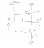
What my pair of devices requires is applying the accelerator to the SIT.
A re-drawn schematic of my pair of devices is attached. The Vgs values are for power supplies of + / - 24V at Ids = 1.65A at 48 deg C with zero offset between output and power supplies common.
In the BAF 2016 talk by Nelson, he shows a schematic labeled "DEPLETION / ENHANCEMENT FOLLOWER 2"
That schematic sets the bias of the SIT more negative than the bias of the enhancement MOSFET.
I call this putting the brakes on the SIT.
What my pair of devices requires is applying the accelerator to the SIT.
A re-drawn schematic of my pair of devices is attached. The Vgs values are for power supplies of + / - 24V at Ids = 1.65A at 48 deg C with zero offset between output and power supplies common.
Attachments
Last edited:
Hi woofertester, take a look at post #108/DEF Amp. I think function 3 also adapts to Vgs of the PMos more negative of NJ.
Hi woofertester, take a look at post #108/DEF Amp. I think function 3 also adapts to Vgs of the PMos more negative of NJ.
It looks to me that his SIT gate was more negative than his PMOS gate in all of the schematics on that page.
Yes, it's true, I wanted to say that yours too string resistances with Vgs PMos > Vgs NJ, in absolute value, adjusts the output offset.
This is may last DEF experiment. There is the most negative FET enhancements mode. Before reaching a stable offset, Vos went up and then back down.
This is may last DEF experiment. There is the most negative FET enhancements mode. Before reaching a stable offset, Vos went up and then back down.
I find that the output stage when cold has 150 mV of offset. The output stage is set for 0v offset at 50 deg C.
The offset is definitely dependent on temperature
My guess is that a resistor array with one or more thermistors can reduce the drift of offset over temperature.
A very gentle DC servo may be worth investigating.
My initial desire is to use this as a DC coupled follower much like an F4.
For the pair of devices that I am using, 67 mV is the difference between the two gate voltages.
I care about DC offset when in temp equilibrium
while arriving there , I don't care even for 1V5 , it'll not harm even hysterical Lowthers and such , under sole condition that nothing is abrupt
while arriving there , I don't care even for 1V5 , it'll not harm even hysterical Lowthers and such , under sole condition that nothing is abrupt
I care about DC offset when in temp equilibrium
while arriving there , I don't care even for 1V5 , it'll not harm even hysterical Lowthers and such , under sole condition that nothing is abrupt
Good to know. I will not worry about it then.
If laying out a PCB, it should be simple to have a network and and a couple of jumpers that will handle the cases of SIT Vgs being either low or higher than P-FET Vgs.
Hi Woofertester, I am following your experiments with great interest.
Perhaps you can do without the resistors string with the Vgs voltage difference between the SIT and the P-FET is less than 200mV.
Antoinel, what do you make of this?
Sorry claudio52 for not catching this post in time.
Best
Anton
...
I am satisfied that if the SITs are well matched and the P-FETs are well matched, it should be possible to put together sets of quad devices to make a stereo amp. Both channels should bias up nearly identically.
...
Hi Woofy,
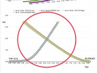
I cloned the SIT-3 with BUZ905D and THF-51S.
Without any source’s resistor, Ids and Vgs were traced and graphed.
Thanks and have a nice Noël to you and “others SIT die hard”
Regards
Pascal
Attachments
Hi Woofy,
I cloned the SIT-3 with BUZ905D and THF-51S.
Without any source’s resistor, Ids and Vgs were traced and graphed.
Thanks and have a nice Noël to you and “others SIT die hard”
Regards
Pascal
Very nice job. The Tokin SIT parts in my possession have Vgs > 3V for Ids = 2A.
For a typical DIY scenario, funds are limited, the amount of parts available are limited and your test equipment available are limited.
Nelson's #2 schematic of the DEF amp is the best way to bias a DIY DEF pair.
One problem that you have to account for is that the temp coefficient of the Tokin SIT is positive whereas the SIT used by Nelson in DEFiSIT has a negative temp coefficient. You have run the Tokin DEF pair to 50 deg C and make your final bias adjustments at 50 deg C.
More to follow as I get a final setup for a DEF pair that look good enough to deploy in an amp.
While SIT stands for something outstanding, a hodgepodge of various kinds of devices go by the name of SIT. I, in the discussions, have difficulty discerning any technical or qualitative differentiation...
Just as with other transistors or tubes - variety in the specific character.
SITs are junction field effect transistors (Jfet) except that they have a broad
"linear region" in their characteristic, much like Triodes. Everything else is
more like a Pentode, where the curves flatten out as voltage increases.
SITs are junction field effect transistors (Jfet) except that they have a broad
"linear region" in their characteristic, much like Triodes. Everything else is
more like a Pentode, where the curves flatten out as voltage increases.
The name SIT has been the source of great confusion. Only certain depletion mode devices with a high cutoff voltage will display the distinctive character. These V(groove)FETs have a vertical structure and an insulated gate while JFETs have a gate-channel P-N junction diode.
The name SIT has been the source of great confusion. Only certain depletion mode devices with a high cutoff voltage will display the distinctive character. These V(groove)FETs have a vertical structure and an insulated gate while JFETs have a gate-channel P-N junction diode.
Define "high cutoff voltage" enough so that it can be objectively measured.
- Home
- Amplifiers
- Pass Labs
- Tokin SIT DEFiSIT musings