Here's an example. I grabbed seven J109s from my parts box. Four from a Mouser buy with spread-out 0.1" leads in cut tape format, three from a DigiKey buy in bulk with leads not spread-out.
Having NO CLUE about your required current I just installed a fixed source resistor of 560 ohms in every case. Then I measured the current of the JFET+resistor circuit. Keep in mind that the (max/min) ratio of IDSS is 5.0, i.e. 500 percent. But the source resistor provides negative feedback that reduces the variability.
The average current of these seven (NJFET + R) sources, was 5.52 milliamps. The deviations from average are shown in this spreadsheet:
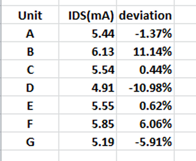
Not bad! The negative feedback resistor in the source leg, reduced the variation to less than 15 percent.
The "knee voltage" at which the JFET+R becomes a current source, was 2.9 volts. As long as the applied voltage exceeds 2.9 volts, this two element circuit behaved as a current source: current = constant, independent of voltage.
Having NO CLUE about your required current I just installed a fixed source resistor of 560 ohms in every case. Then I measured the current of the JFET+resistor circuit. Keep in mind that the (max/min) ratio of IDSS is 5.0, i.e. 500 percent. But the source resistor provides negative feedback that reduces the variability.
The average current of these seven (NJFET + R) sources, was 5.52 milliamps. The deviations from average are shown in this spreadsheet:
Not bad! The negative feedback resistor in the source leg, reduced the variation to less than 15 percent.
The "knee voltage" at which the JFET+R becomes a current source, was 2.9 volts. As long as the applied voltage exceeds 2.9 volts, this two element circuit behaved as a current source: current = constant, independent of voltage.
Attachments
Last edited:
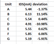
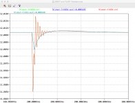
Here is one of them. A J109 with 560R in the source leg, on my protoboard.
1 volt/div horizontal
1 mA/div vertical
On this one the "knee" is at about 3.3V. Output current is 5.6 to 5.7 mA and it's a pretty good current source: current vs voltage is flat, with very little slope.
_
1 volt/div horizontal
1 mA/div vertical
On this one the "knee" is at about 3.3V. Output current is 5.6 to 5.7 mA and it's a pretty good current source: current vs voltage is flat, with very little slope.
_
Attachments
I recall that you had trouble before when you used the IDSS of a MMBF5460 as your current reference. Datasheet says: 1mA to 5mA but LTSPICE model disagrees. LTSPICE model is wrong-ola.
Ooh. You are right. I switched to using an MMBFJ176 and measured Idss of my batch of samples at around 9mA. I updated my BoM, but forgot to update the circuit in Eagle which I used as a template for this.
I recommend you switch to MMBFJ108 or PMBFJ109 + source resistor. I have a dozen of each, in thru hole, and can do a quick protoboard measurement to find the right resistor value that gives the current you want. Just tell me (a) which NJFET you will use; (b) what current you want. I'll figure out the right resistor value.
Then, as before, you can verify that you're getting ZACKLY the current you want in your final product, by measuring the voltage across R5 (post#61) with a digital voltmeter. Ohm's Law tells you the current.
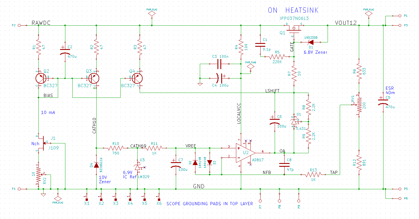
Would this not be more important in the construction where Vref (and the op amp supply) are driven from Vin? There a constant current through the Vref zeners/voltage references (that circuit used a Zener as a pre-reg before the LM329) was even more important plus the current source was feeding two Vrefs and the level shifter. Here (in this simplified construction) it is just feeding the level shifter - in my case an LM4040AIM 5.0. A sample measuring 9mA seemed ok.
PS: Hmm I just noticed the Ein of the LM4040. Not particularly low noise at 35uV. Perhaps it would be beneficial to switch to a TL431 in SOT-23-3 although I'll need two more resistors to shift 5V.
Or better yet, an SPX431L... But then again there's next to no current flowing from gate to sources maybe it doesn't matter (in contrast to a BJT pass transistor)
Last edited:
Another point, why the focus on a low impedance level shifter when you have to slap a 10-22 Ohm resistor between the shifter and the gate of the pass transistor?
The opamp's output voltage is level-shifted up by 5.0 volts, using a TL431 as a low impedance 5V zener. A constant current of 10mA (from Q4) flows in the level shifter, ensuring it remains a low impedance.
You want the external current to be large enough to put the VREF "diode" solidly beyond its min-current-to-regulate knee (a big number for the TL431 and its cousins). AND you want the external current to put the output stage of the error amplifier solidly into class-A operation. For an AD817 I'd suggest 10mA. That might be slightly worrisome with an LM4040 whose Imax is only 20mA; happily, the TL431 can drink 100mA all day long.
As for reducing or eliminating the capacitor across the reference "diode" -- try it in simulation and see. Run .AC analysis to see its impact upon bandwidth and phase margin; and run .NOISE analysis to see how much or how little it attenuates reference noise.
By the way, your gate oxide protection zener D9 is configured unusually. The way you have it, the regulated output voltage cannot exceed (VD9 - VTHnmos). Since VTHnmos is big and not well controllled, you may not be able to crank the output voltage above 15.5 volts or thereabouts. Which is fine if the target is 10V, but maybe not so good if the target is "experiment with a variety of opamps including the NE5532, which is rated for ±22V absolute maximum and which happily runs at ±19V all day long"
Perhaps I am missing something but... Let's say the current source is delivering 10mA (9mA and change in my case with my samples of MMBFJ176). There's next to no current flowing through the MOSFET gate. So the AD817 just needs to sink the current source current and charge and discharge the gate capacitance to regulate Vout. Do you really think the latter is going to exceed 5mA and push the LM4040 beyond its recommended operating range?
|| I'm a bit confused as to how to look at this in LTspice. We'd need an AC small signal voltage source at the input and look at the current flowing in the time domain (transient analysis) but as I understand it such small signal AC source is ignored in an AC analysis. ||
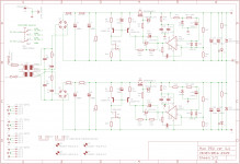
"capacitor across the reference diode" - which do you mean? Your C6 is my C11 (C12) and in your C7 is my C17 (C18). (Your circuit copied below for reference.) I understand that the C6 cap is needed to bypass small signal AC from op amp to MOSFET gate and according to the TL431 data sheet Fig 16 anything larger than about 3uF serves to keep the TL431 stable. You found it necessary to reduce C6 from 180u to 100u for stability reasons? Sorry, I'm confused at to what you mean.
Regarding the gate oxide protection resistor, this is how it is configured in my 12V, 5V and 3V3 circuits from my "adventures with 5A regulated voltage circuits thread". Looks like I followed your advice here
I used an 18V Zener. I can, of course, make the change here easily and achieve greater board flexibility.
|| I'm a bit confused as to how to look at this in LTspice. We'd need an AC small signal voltage source at the input and look at the current flowing in the time domain (transient analysis) but as I understand it such small signal AC source is ignored in an AC analysis. ||
"capacitor across the reference diode" - which do you mean? Your C6 is my C11 (C12) and in your C7 is my C17 (C18). (Your circuit copied below for reference.) I understand that the C6 cap is needed to bypass small signal AC from op amp to MOSFET gate and according to the TL431 data sheet Fig 16 anything larger than about 3uF serves to keep the TL431 stable. You found it necessary to reduce C6 from 180u to 100u for stability reasons? Sorry, I'm confused at to what you mean.
Regarding the gate oxide protection resistor, this is how it is configured in my 12V, 5V and 3V3 circuits from my "adventures with 5A regulated voltage circuits thread". Looks like I followed your advice here
Notice that if you used a 2W or greater zener, you could simply connect a single zener to ground from the MOSFET gate node. If its zener voltage is more than 15V but less than 20V, it won't turn on during normal operation with Vout=12V, but it will prevent Vgate from exceeding Vzener.
I used an 18V Zener. I can, of course, make the change here easily and achieve greater board flexibility.
Last edited:
If you are interested in studying what happens when you increase the impedance from opamp output pin, to MOSFET gate, one way to do that is to decrease the capacitance in parallel with the level shifter "diode" and run whatever simulations you normally run, to see whether your-favorite-metrics get worse, better, or stay the same. If you prefer to study it by changing something other than the parallel capacitor, feel free.
10mA thru a 20mA-rated LM4040 is probably just fine; but the margin-of-safety is even higher when you push 10mA thru a 100mA-rated TL431. Some people always choose the option with the largest margin-of-safety; other people scoff when they perceive overabundant / embarrassing conservatism.
I'm saddened to learn that this supply, which I understand is supposed to power opamp-based analog circuitry and not +12V digital circuits inside a music server PC, is going to have fixed plus-or-minus twelve volt outputs. Some opamps get better and better the more supply volts you give them and twelve volts is not even close to the upper limit for the really good ones. Leaving yourself the option to try this someday, seems worthwhile IMO.
Regarding "tell me the answer" types of questions, I don't care for them. I prefer "critique my thoughtful analysis" instead.
10mA thru a 20mA-rated LM4040 is probably just fine; but the margin-of-safety is even higher when you push 10mA thru a 100mA-rated TL431. Some people always choose the option with the largest margin-of-safety; other people scoff when they perceive overabundant / embarrassing conservatism.
Ok. I agree with your last point. I was just worried about the circuits I already have in use with the LM4040AIM. (My ATX power supply and headphone amp +/-12V supply.) Those LM4040 haven't blown yet. I agree that the TL431 provides more margin-of-safety.
I'm saddened to learn that this supply, which I understand is supposed to power opamp-based analog circuitry and not +12V digital circuits inside a music server PC, is going to have fixed plus-or-minus twelve volt outputs. Some opamps get better and better the more supply volts you give them and twelve volts is not even close to the upper limit for the really good ones. Leaving yourself the option to try this someday, seems worthwhile IMO.
No, I intended this to be more flexible (with the change of Rx). The gate protection diode was a good catch. Thanks!
Regarding "tell me the answer" types of questions, I don't care for them. I prefer "critique my thoughtful analysis" instead.
I agree, but in this case it wasn't clear to me what you were saying. I'll look more closely at the impact of changing C11/12.
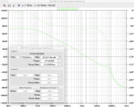
My model has been using an LT1634-5 for the level shifter, given I could not find a model for the LM4040AIM. Varying C11, the capacitor parallel to the level shift voltage reference, has virtually no impact on gain and phase margin, transients or line rejection. .NOISE analysis suggests lowering the size of the capacitor from 180u to 100u reduces output noise very slightly around 200Hz or so (see attached which measures noise at Vout with reference to Vin - I think I am expressing that correctly).
I'll now take a look at this in the context of replacing the LM4040 with a TL431...
(My model is still running a MMBF5460. I need to try to find a model for the MMBFJ176. I could not find one on the Fairchild website.)
I'll now take a look at this in the context of replacing the LM4040 with a TL431...
(My model is still running a MMBF5460. I need to try to find a model for the MMBFJ176. I could not find one on the Fairchild website.)
Attachments
Last edited:
This website has something. No idea how wrong it is.
http://web.rfoe.net:8000/ZILIAOXIAZAI/PHILIPS/models/spicespar/data/j174.html
This other website has something too, Equally no idea about trustworthiness.
Standard.jft - LTwiki-Wiki for LTspice
http://web.rfoe.net:8000/ZILIAOXIAZAI/PHILIPS/models/spicespar/data/j174.html
This other website has something too, Equally no idea about trustworthiness.
Standard.jft - LTwiki-Wiki for LTspice
Well I have spent the better part of the last 24 hours modelling in LTspice. Some interesting results, including some surprises.
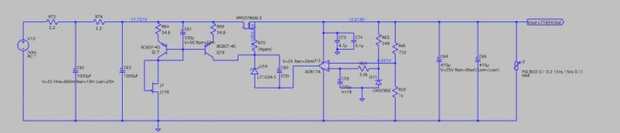
A few of the easy points first. I ran 4 sets of models: one using the TL431 setup (with 2x 2.2k resistors to provide a 5V level shift) and another set using the LT1634-5 I had modelled with previously - each with op amps and Vref driven from Vin (in a setup similar to Mark's circuit but using the components I had initially used to build my prototype for my old project) and also driven from Vout (with it's lower component count). Both sets, the "TL431 level shift" set and the "LT1634 level shift" set, produced the same results for line rejection, phase and gain margin, and transients. There was no sensitivity to speak of to the capacitor parallel to the level shifter. The modelling popped up a bunch of issues however.
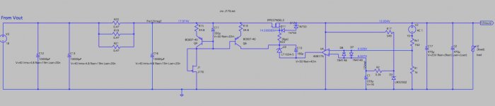
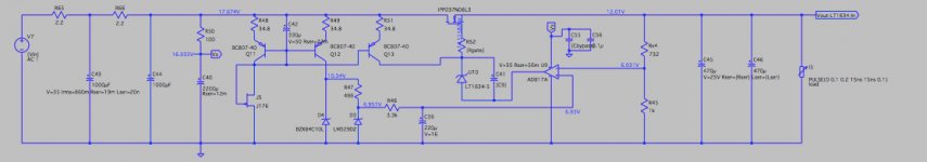
My previous project with this circuit was designed to handle currents of up to 5A and had much more capacitance (and less resistance) upfront. Initially, as noted previously, the circuit was designed to power the AD817A op amp and Vref network from Vin a la Mark's circuit. Later, I changed it to one driven from Vout a la the Jung/Didden regulator. Before making this change I adapted my model in LTspice and checked phase and gain margin. All looked good and eventually the physical circuit performed well in transient testing. (LTspice circuit and output in pics 1 and 2 attached. I changed the model from an MMBF5460 to the J176. It did not affect the output.)
Until now I was thinking I could just change the 'front end' CRC filter network and keep the 'back end' IPP037N network as is for this lower-current project. But with Mark's prompting I went back to my Spice models and revamped them to better match this project. Pics 3 and 4 are the LT1634 level shift versions of the models. (Rser =30m and Lser = 4.5n) I added into the analysis the 0.1u and 4.7u bypass caps in the actual circuit...
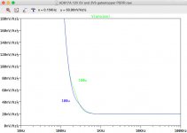
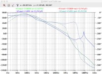
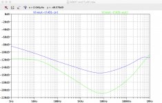
An analysis of phase and gain margin threw up some curve balls. Pic 5. With no phase margin it was no surprise to see the 'powered from Vout' versions oscillate in a transient analysis. The 'powered from Vin' versions performed much better, but the peak in the gain back above unity looks ugly and there was still some 'noise' for a short period immediately after the initial transient waveform.
Comparing pics 1 and 4, there aren't many differences. Omission of the diode protection networks doesn't make a difference. I updated a few of the component values (e.g. voltage ratings) but none of these changes were significant. The principal differences are just the input filter and bypass caps.
If I add the bypass caps into my old project model modelled phase margin is destroyed as they effectively parallel the output caps and shift the output pole dramatically. Given these bypass caps are used to prevent HF interaction with parasitic components in the real circuit, which aren't modelled, am I right to conclude that modelling the bypass caps is a bad idea?
Removing the bypass caps from this project's models has a profound impact on the 'powered from Vout' version (unsurprisingly, for the reason given above). Pic 6. But the hockey stick gain profile remains. Is this to be feared? Artefacts in the transient analysis suggest so. Initial analysis suggests I would benefit from a lot more capacitance in the initial filter network to knock out this hockey stick...
I'll leave my analysis at this for now, mostly out of fear that I would have to retype it all if I something goes wrong posting.
A few of the easy points first. I ran 4 sets of models: one using the TL431 setup (with 2x 2.2k resistors to provide a 5V level shift) and another set using the LT1634-5 I had modelled with previously - each with op amps and Vref driven from Vin (in a setup similar to Mark's circuit but using the components I had initially used to build my prototype for my old project) and also driven from Vout (with it's lower component count). Both sets, the "TL431 level shift" set and the "LT1634 level shift" set, produced the same results for line rejection, phase and gain margin, and transients. There was no sensitivity to speak of to the capacitor parallel to the level shifter. The modelling popped up a bunch of issues however.
My previous project with this circuit was designed to handle currents of up to 5A and had much more capacitance (and less resistance) upfront. Initially, as noted previously, the circuit was designed to power the AD817A op amp and Vref network from Vin a la Mark's circuit. Later, I changed it to one driven from Vout a la the Jung/Didden regulator. Before making this change I adapted my model in LTspice and checked phase and gain margin. All looked good and eventually the physical circuit performed well in transient testing. (LTspice circuit and output in pics 1 and 2 attached. I changed the model from an MMBF5460 to the J176. It did not affect the output.)
Until now I was thinking I could just change the 'front end' CRC filter network and keep the 'back end' IPP037N network as is for this lower-current project. But with Mark's prompting I went back to my Spice models and revamped them to better match this project. Pics 3 and 4 are the LT1634 level shift versions of the models. (Rser =30m and Lser = 4.5n) I added into the analysis the 0.1u and 4.7u bypass caps in the actual circuit...
An analysis of phase and gain margin threw up some curve balls. Pic 5. With no phase margin it was no surprise to see the 'powered from Vout' versions oscillate in a transient analysis. The 'powered from Vin' versions performed much better, but the peak in the gain back above unity looks ugly and there was still some 'noise' for a short period immediately after the initial transient waveform.
Comparing pics 1 and 4, there aren't many differences. Omission of the diode protection networks doesn't make a difference. I updated a few of the component values (e.g. voltage ratings) but none of these changes were significant. The principal differences are just the input filter and bypass caps.
If I add the bypass caps into my old project model modelled phase margin is destroyed as they effectively parallel the output caps and shift the output pole dramatically. Given these bypass caps are used to prevent HF interaction with parasitic components in the real circuit, which aren't modelled, am I right to conclude that modelling the bypass caps is a bad idea?
Removing the bypass caps from this project's models has a profound impact on the 'powered from Vout' version (unsurprisingly, for the reason given above). Pic 6. But the hockey stick gain profile remains. Is this to be feared? Artefacts in the transient analysis suggest so. Initial analysis suggests I would benefit from a lot more capacitance in the initial filter network to knock out this hockey stick...
I'll leave my analysis at this for now, mostly out of fear that I would have to retype it all if I something goes wrong posting.
Attachments

Didn't read the wall of text / too much effort required.
I sort of get the impression you are (re)discovering that a voltage regulator made of a source follower and a very high gain-bandwidth error amplifier, is supremely sensitive to "the output pole" and to the ESR + ESL of all capacitors attached to the output. All capacitors attached to the output.
You could devise a set of simulation experiments whose goal is to discover whether or not ESR+ESL is important in your new voltage regulator, and if it is, to find the location of "the cliff of death" so you can stay a safe distance away. You might wind up installing explicit series resistors, or specifying one certain capacitor part# whose ESR is known and constant, or ...
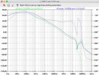
That I understood. I was grappling with two issues. One was modelling bypass caps which affected modelled phase margin (for reasons we've each mentioned) but which seemed not to bother the performance of the physical circuit which was tested.
The other issue was coming from the input which I did not understand at all. I just now found the cause of that problem. I had foolishly left a small signal AC of value 1 on the input voltage when preparing my phase and gain margin .AC analysis. This was creating the positive going "hook" in the gain profile in pics 5 and 6 above. Doof. Revised - no bypass caps - phase and gain margin attached.
(Incidentally the J176 is delivering about 20mA in the model. I guess I could add a source resistor to fine tune the current source to c10mA for modelling purposes to better represent the actual circuit. It may not even make a difference.)
Attachments
No and it need only be 50-100 mOhms. Trace resistance and ESR probably did the job for the previously built circuit. Thx.
Last edited:
I added a 100 mOhm resistor in series with the 'powered by Vout' bypass caps. The 'powered by Vin' bypass caps benefit from the 100R resistor of the RC filtering the Vin to the op amp. It's interesting to now compare the transient response of the 'powered from Vin' versus 'powered by Vout' options. The Vout version seems to perform much better. (I adjusted the relative levels to better align the plots.)
Attachments
Last edited:
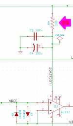
An update. Following Mark's good advice I split the input filter resistors (this showed good improvement in modelling), changed snubber caps C3 and C4 to 1u, added provision to use a higher Idss N-channel FET - I'm thinking of using the MMBFJ108 (SSOT 3L) - and changed the level shifter to provide more current sink flexibility with a 'new-generation' SPX431A. (I believe the TL431 is also available in this SOT89 package.) The gate protection has been fixed also, plus there is the added resistor in series with the op amp bypass caps.
I have a few things to check over still but any comments/advice are very welcome.
Mark, I note that you tested the LME49710 also. Any notable advantages to trying this in lieu of the AD817? I note the difference in stated GBP but this is dependent on supply in any case (+12V supply => less than 50MHz for the AD817) and there's a multitude of other differences (slew rate etc).
Attachments

Last edited:
My purpose in installing a bunch of different opamps with GBWs from 0.5 MHz to 55 MHz, into the same socket on the same regulator PCB, was to demonstrate that it is possible to achieve good stability over a wide range of opamp types and GBWs, both in theory and in practice. There are plenty of constructors and monkey-see monkey-do copiers who have some kind of voodoo fear of opamp stability, and who insist that opamp X is bad while opamp Y is good, because X oscillated in their PCB but Y did not oscillate. My message to them is: it is possible to design for insensitivity to opamp type, over quite a broad range. Sorry to hear that your board wasn't designed for that.
I don't have any special attachment to one opamp or another for regulator use. ADs are fine, LMEs are fine, OPAs are fine with me. I would avoid devices like the TL071 whose internal schematic on the datasheet shows resistors in series with the output pin (OMG 😱), and I would avoid devices whose output stage can't source or sink ~ 15 mA, but that's about all.
I don't have any special attachment to one opamp or another for regulator use. ADs are fine, LMEs are fine, OPAs are fine with me. I would avoid devices like the TL071 whose internal schematic on the datasheet shows resistors in series with the output pin (OMG 😱), and I would avoid devices whose output stage can't source or sink ~ 15 mA, but that's about all.
Understood Mark. (I left the compensation resistor and cap in place for this same reason, although I realise the configuration is different from yours.)
Regarding your kind offer to determine the source resistor value which leads to 10mA current source output when using an MMBFJ108, I note that the SMD and thru-hole versions have very different Idss according to their data sheet. Do you have the SMD '8 version in your parts box?
Regarding your kind offer to determine the source resistor value which leads to 10mA current source output when using an MMBFJ108, I note that the SMD and thru-hole versions have very different Idss according to their data sheet. Do you have the SMD '8 version in your parts box?
- Status
- Not open for further replies.
- Home
- Amplifiers
- Power Supplies
- Thermal considerations for Fairchild SDIP bridge rectifiers